Dual Isolated Power Meter
2025
Project GitHub RepositoryOver the course of my career, I've spent many hours measuring input voltage, input current, output voltage, and output current while characterizing the efficiency of power supplies. This task is, even at larger companies, typically a manual process. Since my first hardware engineering internship, I've wanted to design a custom board to automate these measurements and to simultaneously record these measurements at a push of a button, so in 2023 I finally put something together.

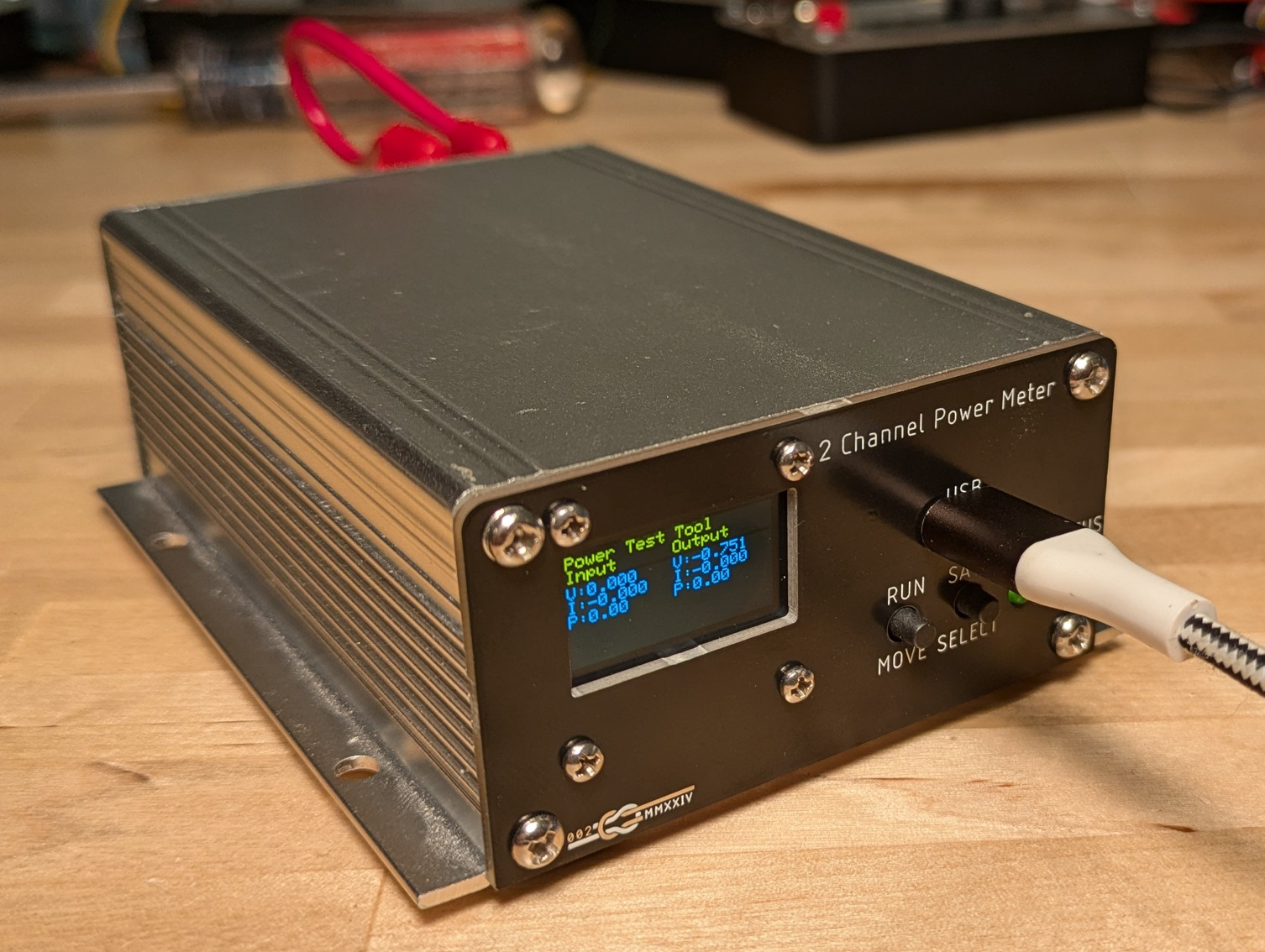
Completed Power Meter
To avoid any weirdness with shared grounds within the meter, both channels are fully galvanically isolated. The parts are rated to 1000V isolation, but since I didn't carefully design to specific creepage rules I would probably not operate this at above 200V common mode to the microcontroller ground.Background
The efficiency of power supplies varies considerably over load, so when validating a design it is necessary to test efficiency at many load conditions. Annoyingly, efficiency also varies with temperature, so you will measure higher efficiency right as you turn a power supply on than you will after everything heats up. To get consistent measurements at a particular temperature, it is best to either have a very good heatsink or to make measurements quickly; when you record measurements by hand, current can drift over the course of making a single measurement. Making the four critical measurements at once: input voltage, input current, output voltage, and output current all nearly instantaneously avoids this issue.
Design
SchematicI reused the form factor of my DNVT Switch for this project but with an ESP32 instead of an RP2040. There is a screen with buttons to initiate measurements on one end, and the power lead inputs are on the other end. I was only able to find one option for stacked right angle banana plugs: The 572 series from Deltron. I was only able to find them on Newark (a great annoyance when I typically order exclusively from Digi-key), and they are annoyingly expensive ($7 each), but they were perfect for this project.
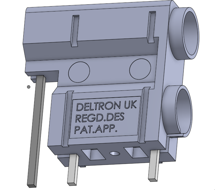
Stacked Banana Plug CAD Model
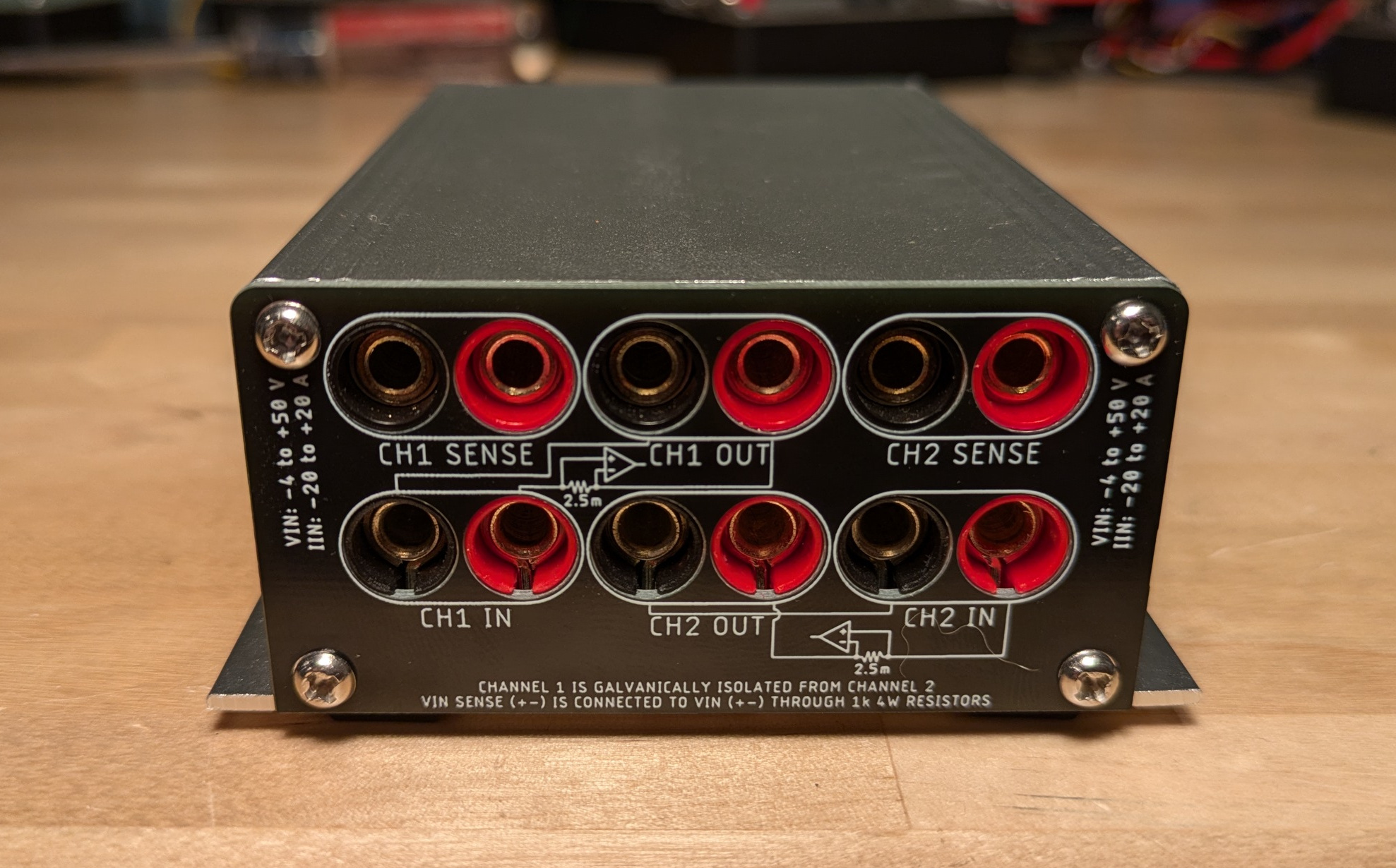
Back Panel
I started with 5V in and 5V output isolated power supplies (as the schematic indicates), but I found that the large voltage ripple from these supplies was corrupting measurements. I anticipated that this might be an issue, so I swapped the 5V in 5V out isolated supplies for 5V in 9V out supplies which I then regulated down to 5V with a high performance ADC. The half rail reference (which allows for negative voltage and current measurements) is supplied by an OPA2333. This could have been just about any OP-AMP, but I was given a reel of these that failed solderability tests and were otherwise going to go into the trash and therefore have a lifetime supply of them.
Voltage sensing is provided by a simple voltage divider off of a remote sense input. There is a 1kΩ resistor tying the power input to the sense input so that a somewhat valid voltage measurement can still be made if the voltage sense input is not separately connected. This 1kΩ resistor is made from 10 separate 100Ω 1206 resistors so that the board is robust to connecting 50V between the sense and power inputs by mistake. 100Ω 1206 resistors are a standard assembly part from JLCPCB, so they are basically free. The voltage sense inputs are not directly connected to the current carrying inputs in order to prevent drop in the current carrying cables from influencing the measurement. In the event that separate voltage sense cables are not available, you should short the current sense input to the voltage sense input to minimize error.
Current sensing is provided by INA240 which is a non-isolated current sense amplifier with a high common mode input voltage. I chose it over a Hall Effect current sensor for accuracy.
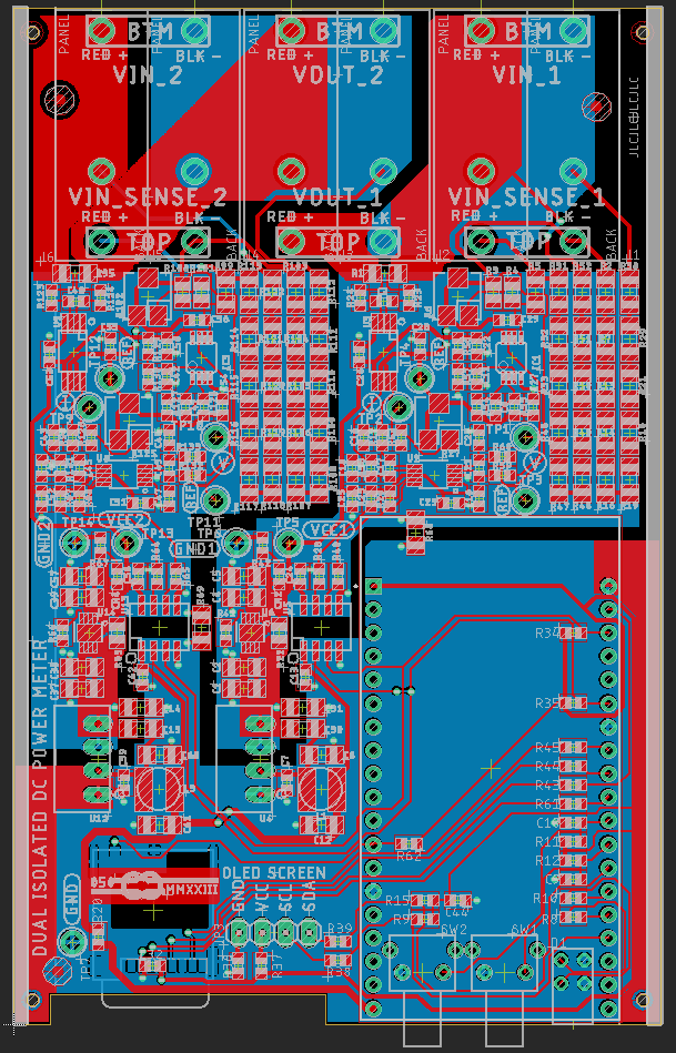
PCB Layout
To bridge the isolation gap between the microcontroller and the two isolated inputs, I use ISO1640BDR. Digital isolators are quite handy for precision isolated sensing circuits like this. It is a magic bridge between two power domains. With a digital isolator, I am able to put a high precision ADC on a floating rail in order to make a precise measurement. This device can sense which end is driving the circuit (by intentionally pulling the side 1 ~650mV above ground rather than all the way to ground when driving) which allows for the necessary bidirectional data transfer. Coincidentally, the typical application example (of an isolated Data Acquisition System) for this isolator includes an ADS1115.
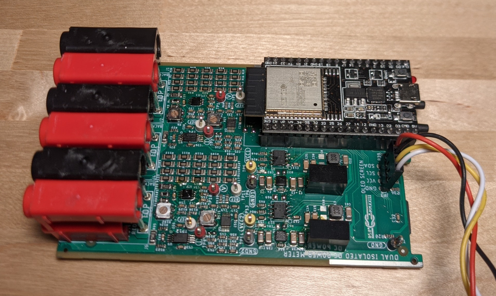
Assembled PCBA
I wrote the software for this project just prior to the advent of generative AI. I selected the ADC that I did because there was an available Adafruit driver, and I selected the ESP32 because it is generally capable and cheap. The code is cobbled together, but it does work. There is a so-far unused micro-SD card on this design which I may look to Generative AI to enable.
The voltage capabilities of ADS1115 are slightly confusing at first glance. The analog input ratings are clear enough—the supply voltage is not to be exceeded, but the range of the PGA is less clear. It shows the possibility of of running at +/- 6.144V, but this is a lie: The inputs cannot go beyond the supply rails.
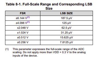
ADS1115 Full Scale Range
Measurements are displayed on a small OLED screen, and a few print panel buttons provide options for user input. As with the DNVT switch, I designed custom end plates for the box to go around all of the connectors.
Bringup
I had JLCPCB assemble most of the parts on the boards but I installed the ADCs and OP-AMPs myself. The ADC was out of stock on Digi-Key and Mouser, so I harvested two from Adafruit eval boards. I was quickly up and running with some test code, but I was concerned by the high output ripple voltage of the isolated DC to DC converters and how that resulted in high ripple on the half rail supply. The isolated DC to DC converters are unregulated and feed through noise on the 5V supply as well. I could see the changing load of the microcontroller in the form of voltage transients on the half rail supply output. While the ADC is differential and this noise should theoretically be removed, I decided to eliminate it by changing the 5V to 5V isolated supplies to 5V to 9V isolated supplies and populating the linear regulators.
With the noise issue resolved, I was still left with a confusing measurement inaccuracy: when the inputs are not connected to anything, -0.75V is measured rather than 0V as you would expect. If the inputs are connected to a low impedance source, there is no error. I puzzled on this for awhile and then shelved the project for a year since this coincided with me moving apartments. When I picked it back up, I went through the circuit node by node trying to find the source of the error. It seemed like the op-amp buffer was the culprit, but I removed a resistor and realized that the issue was coming from the current sense amplifier.
Channel 2 (Marked 'Output') Left Floating
The current sense amplifier works by amplifying a differential voltage across a shunt resistor. Since the supply voltage of the amplifier is less than the maximum voltage sensed, two very well matched resistor dividers (internal to the part) exist before the differential amplifier. These resistors were draying current from the positive sense input and shunting it to ground. Since the half-rail supply is directly tied to the negative sense input, this results in a lower voltage on the positive sense input than on the negative sense input which causes the negative voltage reading. Everything worked fine — this is just a quirk of the circuit.
After correcting my understanding of the circuit, I calibrated the voltage sense by comparing its measurements to the measurements of a Fluke multimeter. My plan had been to fine tune the circuit using the potentiometers, but I didn't have sufficient range. Rather than change out a resistor, I instead put the calibration value in the microcontroller code. This is actually how modern multimeters are calibrated: there are no potentiometers to adjust, just an EEPROM with calibration values. Right now the code is quite basic, but it could be modified to add a web UI calibration mode to allow for these values to be changed.
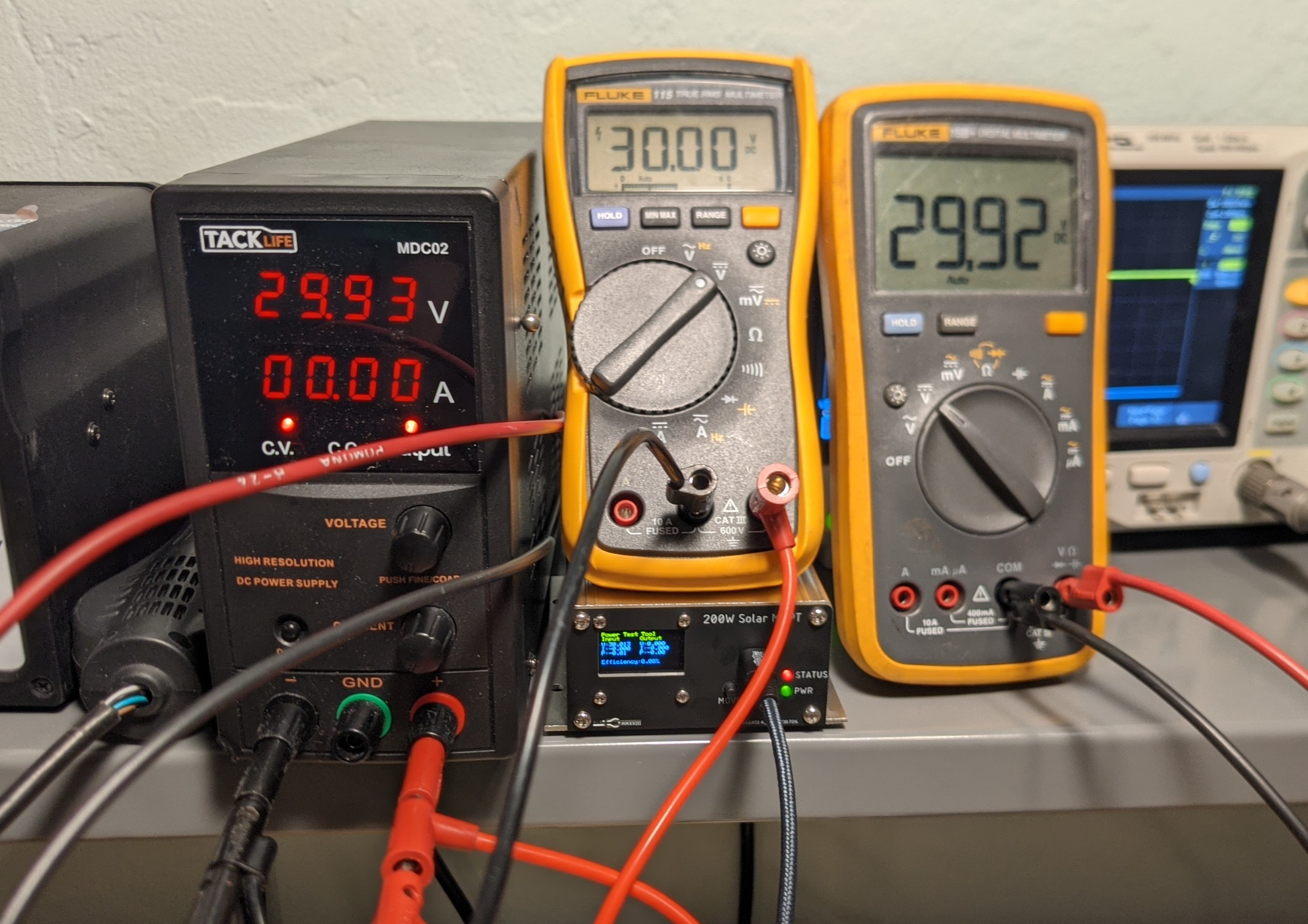
Disagreeing Flukes
This box can be set up for continuous serial logging or for button triggered logging. Each measurement with button triggered logging has an index number based on the number of power cycles the box has been through and the number of times a triggered measurement has been made since the box was last power cycled. The first number is stored in flash and increments on boot while the second number is stored in RAM. This limits the number of flash write cycles.
I haven't brought up any power supplies since wrapping up this project, but I am glad to have it on my shelf ready to go.