Cheap RF Attenuators
2020
EagleCAD FilesFabrication Outputs
I was debugging an old HF transceiver once and needed to measure its transmit waveform at full power. I had a 10W dummy load from Amazon, and I figured that it could handle 50W for a second or two. I was wrong; it immediately burned out. Instead of buying a properly rated dummy load, I decided to build one out of a long chain of attenuators made from 1206 resistors.
The cheapest 50W RF attenuator on Minicircuits is $220. If you lower your standards to Amazon, the price is $67. If you further lower your standards to Ebay, you can score one for $43. On the other hand, I can get ten PCBs from JLC PCB for $2 + shipping. Add in a few hundred resistors at $0.005-$0.025 each, and now you're looking at an attenuator that costs ~$5.
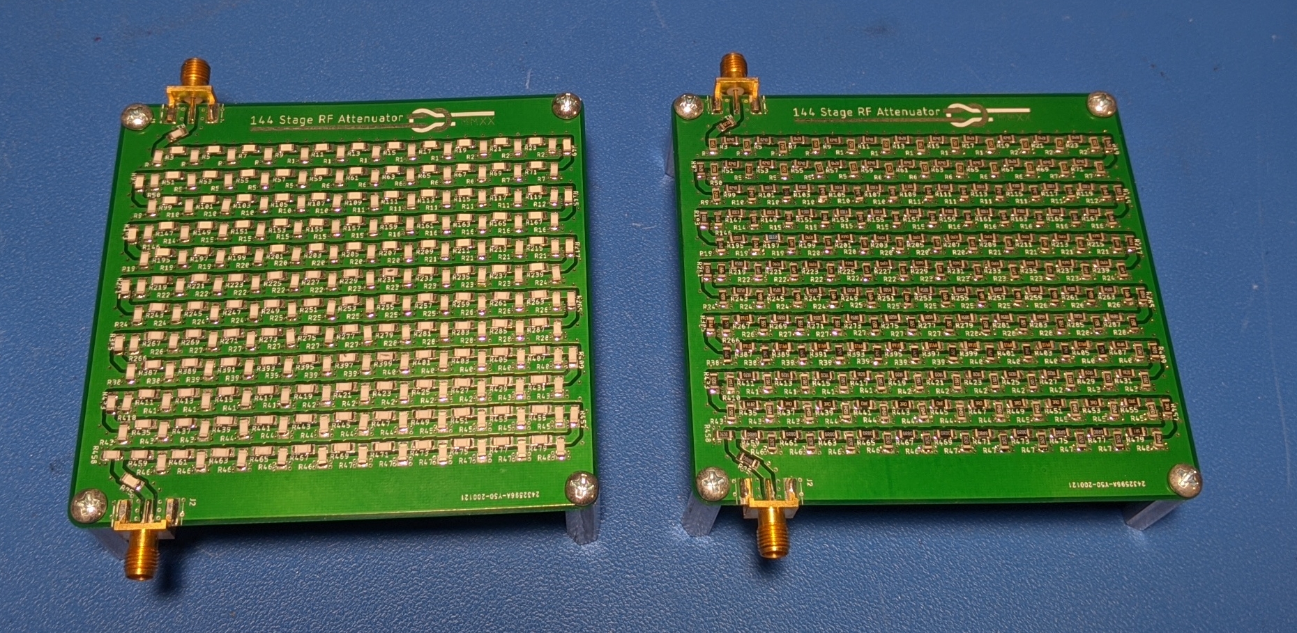
8.5dB Attenuator (left) and 30dB Attenuator (Right)
Design
The design constraints were simple: fit as many stages of attenuators on a 100x100mm (the max size for the $2 JLC deal) as possible. I chose 1206 resistors because their typical power rating is 0.25W, so I would not have to install a ridiculous number of resistors to meet the 50W goal. I chose a two layer 0.6mm thick PCB to keep the trace widths reasonable for 50 ohm lines -- fortunately choosing different thicknesses doesn't change the price. I used 60mil wide traces to match the size of the 1206 pads, but the ideal trace width would have been ~40 mil.
I designed a 12-stage attenuator and then used the Design Block feature of Eagle to duplicate that twelve times which resulted in a 144-stage attenuator:
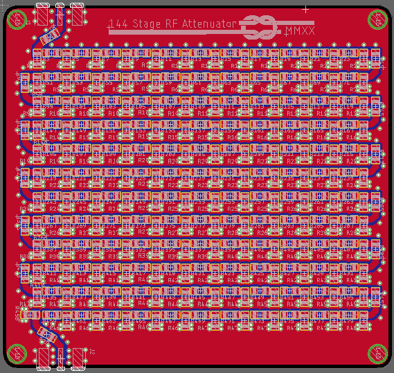
144-stage Attenuator Layout
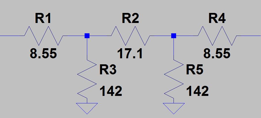
I modeled the T-attenuators in Open Office Calc (here's the sheet) using the equations below:
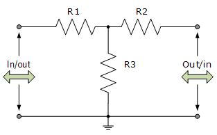
T-attenuator
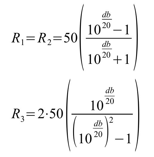
T-attenuator Equations
When you connect two T-attenuators together, you end up with two resistors in series that can just be combined into one resistor with half the value. For example, for a 3dB attenuator you end up with R1=R2=8.55 and R3=142. If you connect two in series to form a 6dB attenuator, the shunt resistors remain the same, but the series resistor in the middle is doubled.
6dB Attenuator
Since the power goes down in each subsequent attenuator stage, the first stages in the chain will consume the most power if the same attenuation is used all stages. This results in some parts getting a lot hotter than others and limits the max input power of the attenuator. To avoid this, the attenuation value needs to increase the further into the chain you get. I chose the points at which to change to new attenuation values somewhat manually using a spreadsheet.
There were three factors to optimize:
- Keep the maximum power dissipation, with a 50W input, below 0.5W in any one stage. Each 'stage' in this design involves two resistors due to the series combination, so limiting each stage to 0.5W will limit per part loss to 0.25W.
- Make good use of each attenuator by not having a lot of stages dissipating a lot less power than others.
- Limit the total number of different attenuation values to make assembly easier and to lower costs by being able to buy a smaller number of different parts in greater bulk.
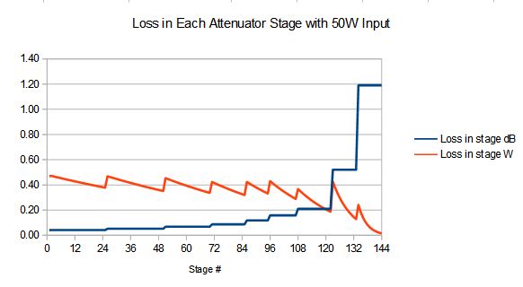
Loss in Each Stage of 30dB Atenuator
I initially assembled just a 30dB attenuator, but I realized I had enough parts on hand to also build an 8.5dB attenuator. As the pictures show, I assembled its resistors upside down in hopes of improving flatness at higher frequency, but it did not seem to have much of an effect and obfuscated the part values meaning that I had to pay a lot more attention in assembly.
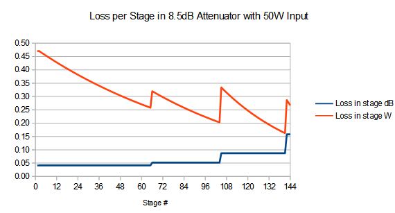
Loss in Each Stage of 8.5dB Attenuator
Measurements
I measured the performance of these attenuators using a NanoVNA V2 Plus by the HCXQS group. Its performance is pretty incredible for <$100 VNA, and its great for working with antennas, filters, and amplifiers as well. The plots below were created by first saving data in the touchstone format using a tool called NanoVNA Saver and then plotting those s-parameters in QUCS.
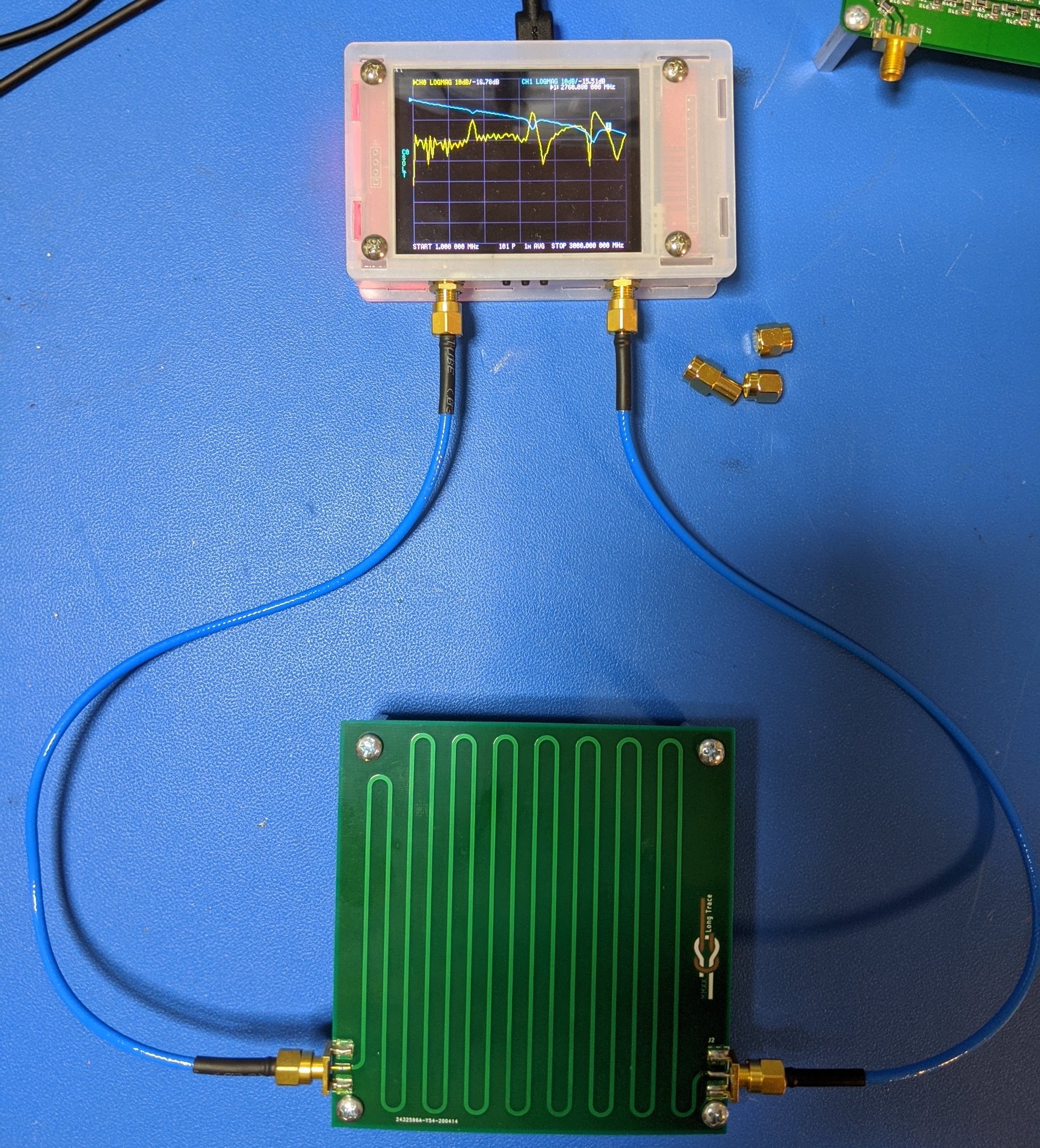
NanoVNA Measuring Trace Loss Test Board
Results
30dB Attenuator s-parameters8.5dB Attenuator s-parameters
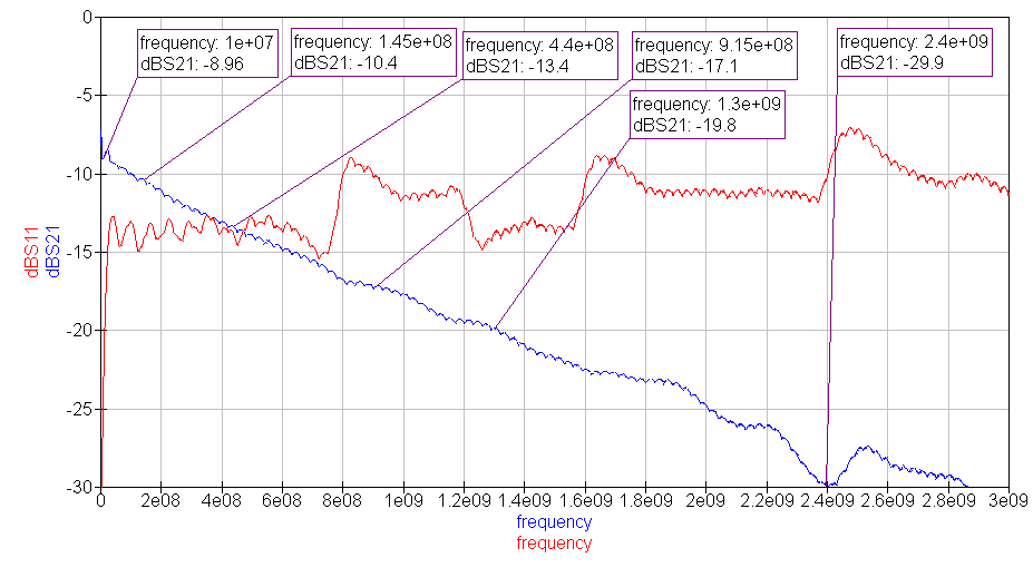
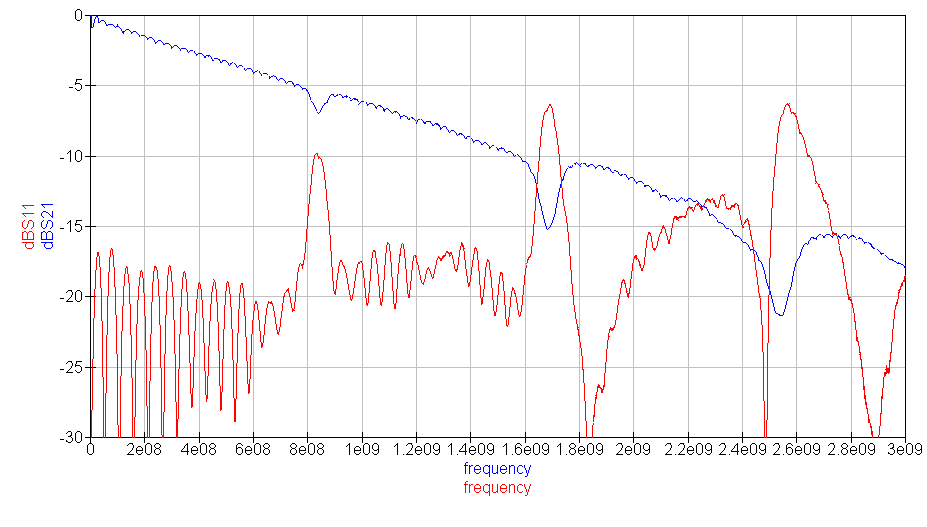
At HF, the attenuators were pretty close to their intended values, but at higher frequencies the loss was higher than the equations would suggest. This was due to frequency dependent losses in the PCB itself as well as frequency dependent increases in the resistance of the resistors due to skin effect. Generic 'FR4' is a very high loss substrate, so it should be no surprise that the attenuators were not flat across frequency. That isn't necessarily an issue, however. You just need to keep the frequency dependency in mind and adjust for the band you are working in.
Overall, this construction method seems to work reasonably well for the 33cm band and below. Since the return loss of the 30dB attenuator is the same with or without termination (an ideal 30dB attenuator has a -60dB insertion loss when unterminated since the reflected power is attenuated again as it passes back toward the source), it can be used as a dummy load in addition to an attenuator.
The boards were in fact able to dissipate 50W, but it would be a good idea to attach a heatsink to the bottom of the board or add a fan to keep that up continuously in order to avoid exceeding the temperature rating of the FR4 laminate.
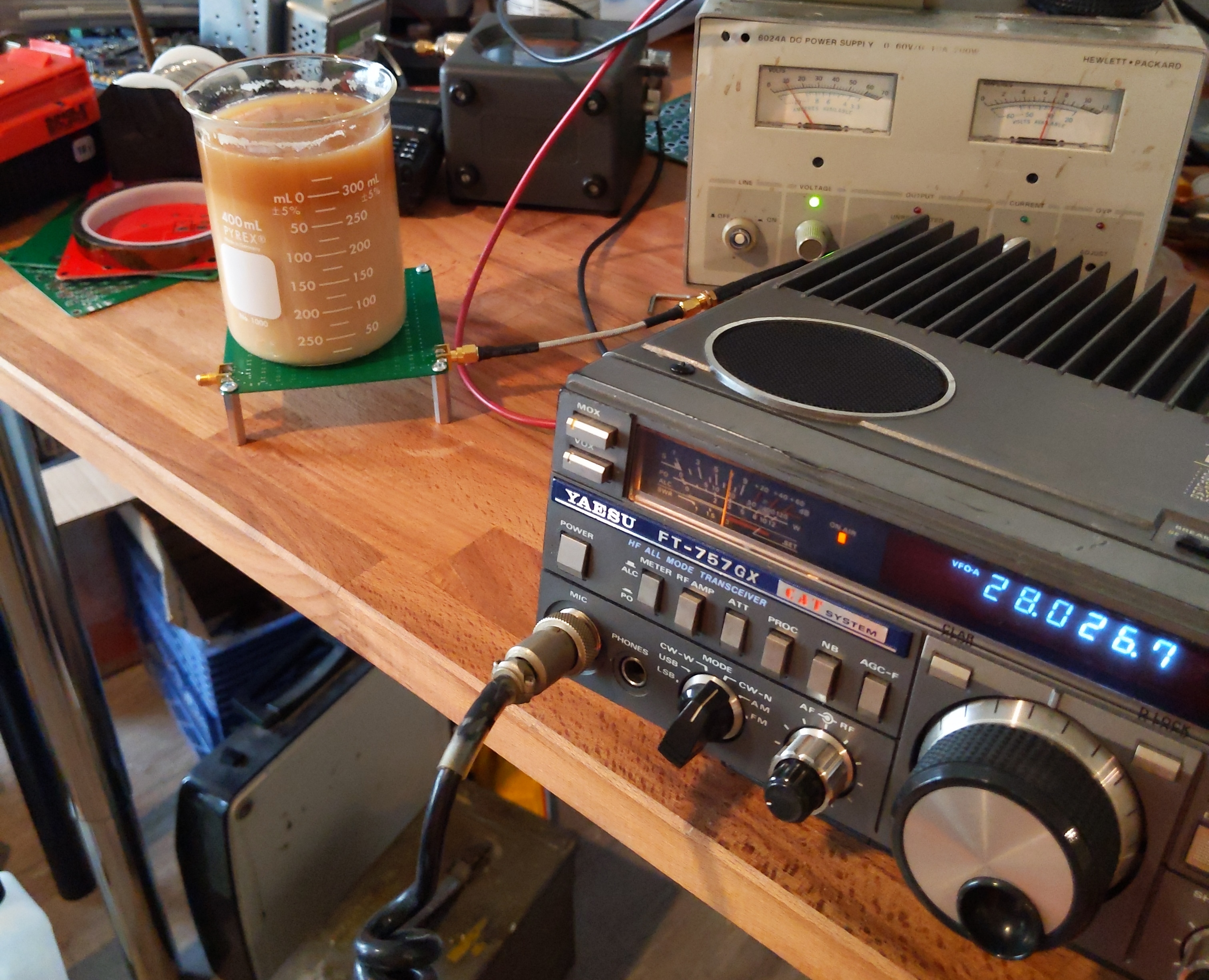
10m Band Coffee Warmer
30dB Attenuator
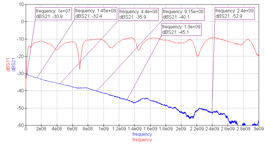
30dB Attenuator Return and Insertion Loss from 1MHz to 3GHz
| Band | Attenuation |
|---|---|
| HF | 30.5dB |
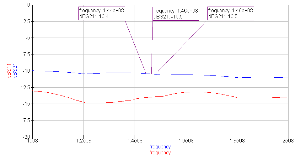
| 2m | 32.5dB |
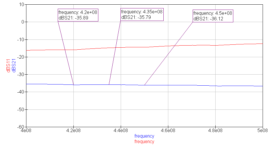
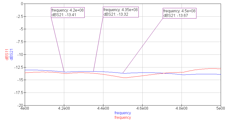
| 70cm | 36dB A |
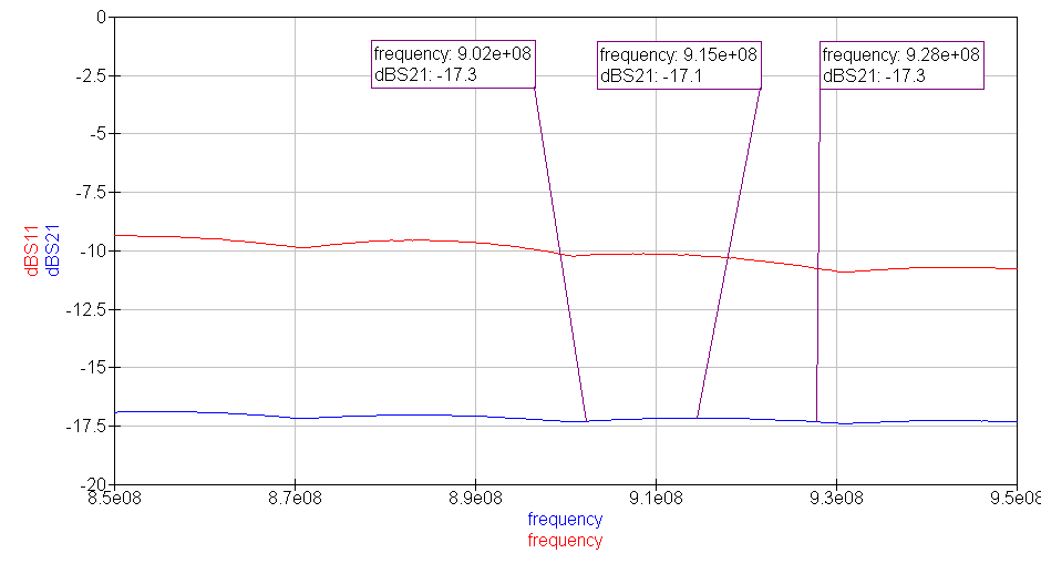
| 33cm | 40dB A |
| 23cm | 45dB A |
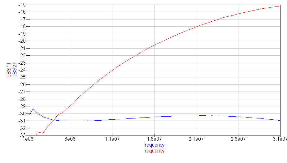
30dB Attenuator Return and Insertion Loss In HF Bands
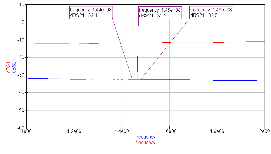
30dB Attenuator Return and Insertion Loss In the 2m Band
30dB Attenuator Return and Insertion Loss In the 70cm Band
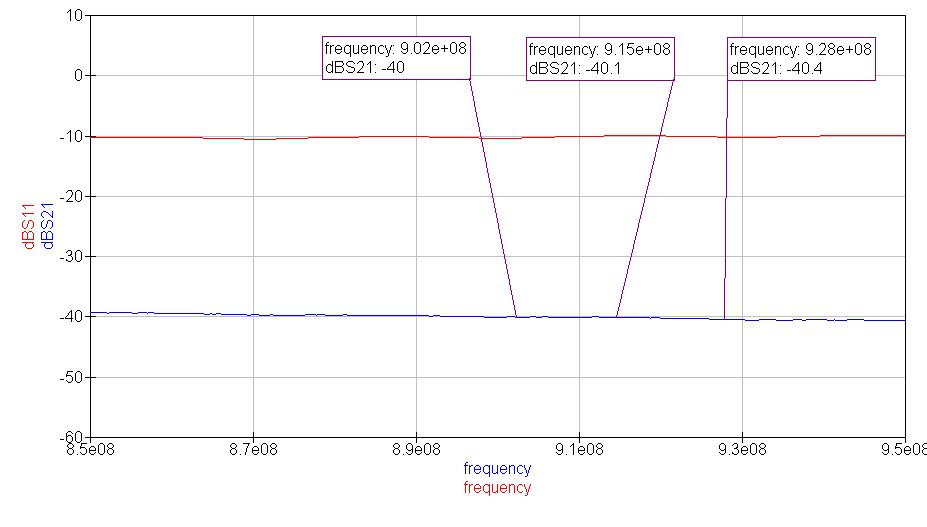
30dB Attenuator Return and Insertion Loss In the 33cm Band
8.5dB Attenuator
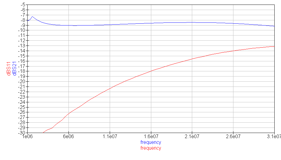
8.5dB Attenuator Return and Insertion Loss from 1MHz to 3GHz
| Band | Attenuation |
|---|---|
| HF | 8.5dB |
| 2m | 10.5dB |
| 70cm | 13.5dB |
| 33cm | 17.2dB |
| 23cm | 20dB |
8.5dB Attenuator Return and Insertion Loss In HF Bands
8.5dB Attenuator Return and Insertion Loss In the 2m Band
8.5dB Attenuator Return and Insertion Loss In the 70cm Band
8.5dB Attenuator Return and Insertion Loss In the 33cm Band
Trace Loss Test Coupon
After seeing how much loss went up with frequency, I decided to make a test board with just one 1.50m long serpentine trace. This board showed two things: The SMA transition for these boards needs to be optimized and there are some weird frequency dependent effects caused by either the serpentine trace coupling to itself or the poor SMA transition.
Long Trace Test Board Return and Insertion Loss
The frequency dependence of the resistors actually seems to be similar to the frequency dependent loss of the PCB itself. I chose cheap thick film resistors for this board, and it is likely that skin effect losses in the restive material of the resistors themselves is the cause. Here's a comparison of the 30dB attenuator board along with the long trace board plus an ideal 30dB attenuator:
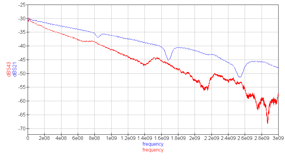
30dB Attenuator (red) vs. Long Trace +30dB Attenuation (blue)
The long trace board has a trace 33% longer than the attenuator board since it has 16 switchbacks vs. the 12 on the attenuator board, so the contribution of the frequency dependent loss in the resistors is even more significant than this plot illustrates.
Using the TDR capability of the VNA, I was able to confirm that, at least under 1GHz, the impedance of the trace is pretty close to 50 Ohms. The velocity factor of the trace is about 0.8 based on these numbers. The jump in impedance at the end even when terminated is another indicator that I need to work on the SMA transition.
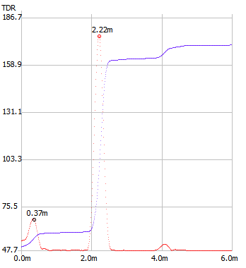
Long Trace Test Board TDR Trace Unterminated 100-900MHz
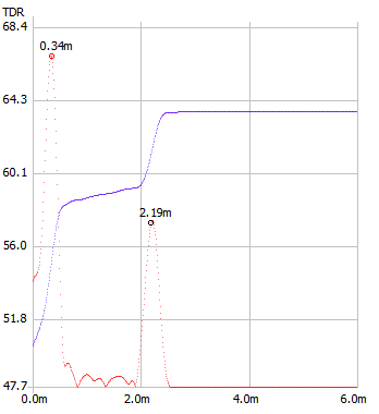
Long Trace Test Board TDR Trace Terminated 100-900MHz
Things go a little crazy when measured from 100-3000MHz. My uninformed speculation is that this is due to coupling effects. The next step here is to design another test coupon with a shorter trace, well stitched top ground pour, and improved SMA transitions.
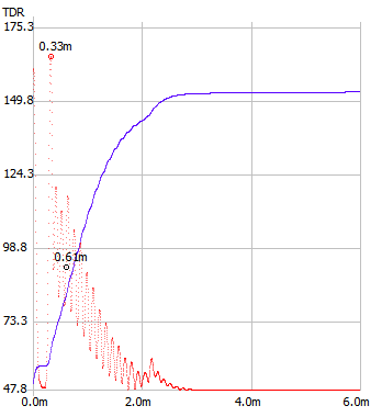
Long Trace Test Board Terminated 100-3000MHz