Scooter Battery USB-C Charger
2022
SchematicLayout
Rev2 EagleCAD Files
Gerbers for Front and Back Panels
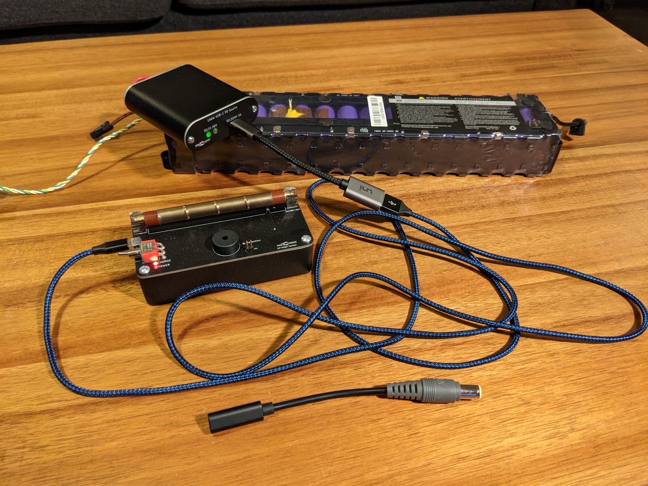
There are plenty of DC input 100W USB-C chargers on the market, but none that I have found support wide input voltage ranges. The goal of this project is to build a USB-C charger with a 20-48V input range that advertises 5, 12, and 20V at up to 100 W. Due to the ubiquity of rental scooters these days, you can pick up used scooter batteries quite cheaply. I purchased a 280 Wh pack from a Xaomi M360 scooter from Jag35 (a company that has capitalized on the fact that there is now a market for used batteries) for something like $35 plus shipping. This charger allows me to use that battery to charge my phone and laptop. Its small and light enough to carry in a backpack but still has some serious capacity at a fraction of the cost of other integrated solutions like Omnichargers.
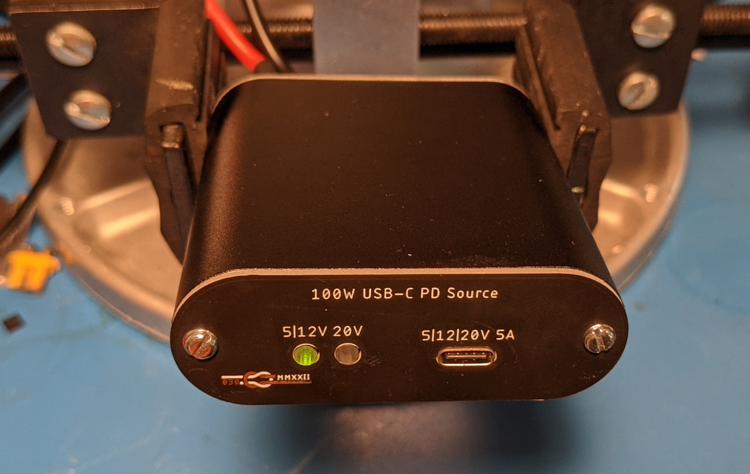
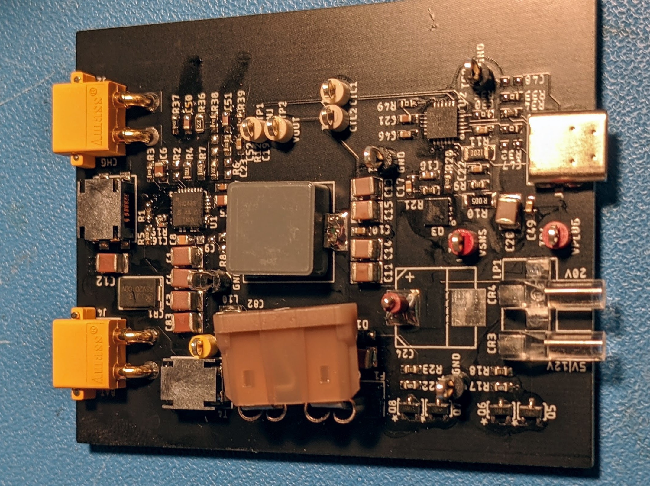
Assembled Charger
This USB PD-Source supports simultaneous charging of the battery it is connected to using a dedicated XT20 charge port, so this could be connected to a solar panel and MPPT for a simple off-grid power solution. With an AC charger on its charge port, it can act as a USB-C Uninterruptible Power Supply.
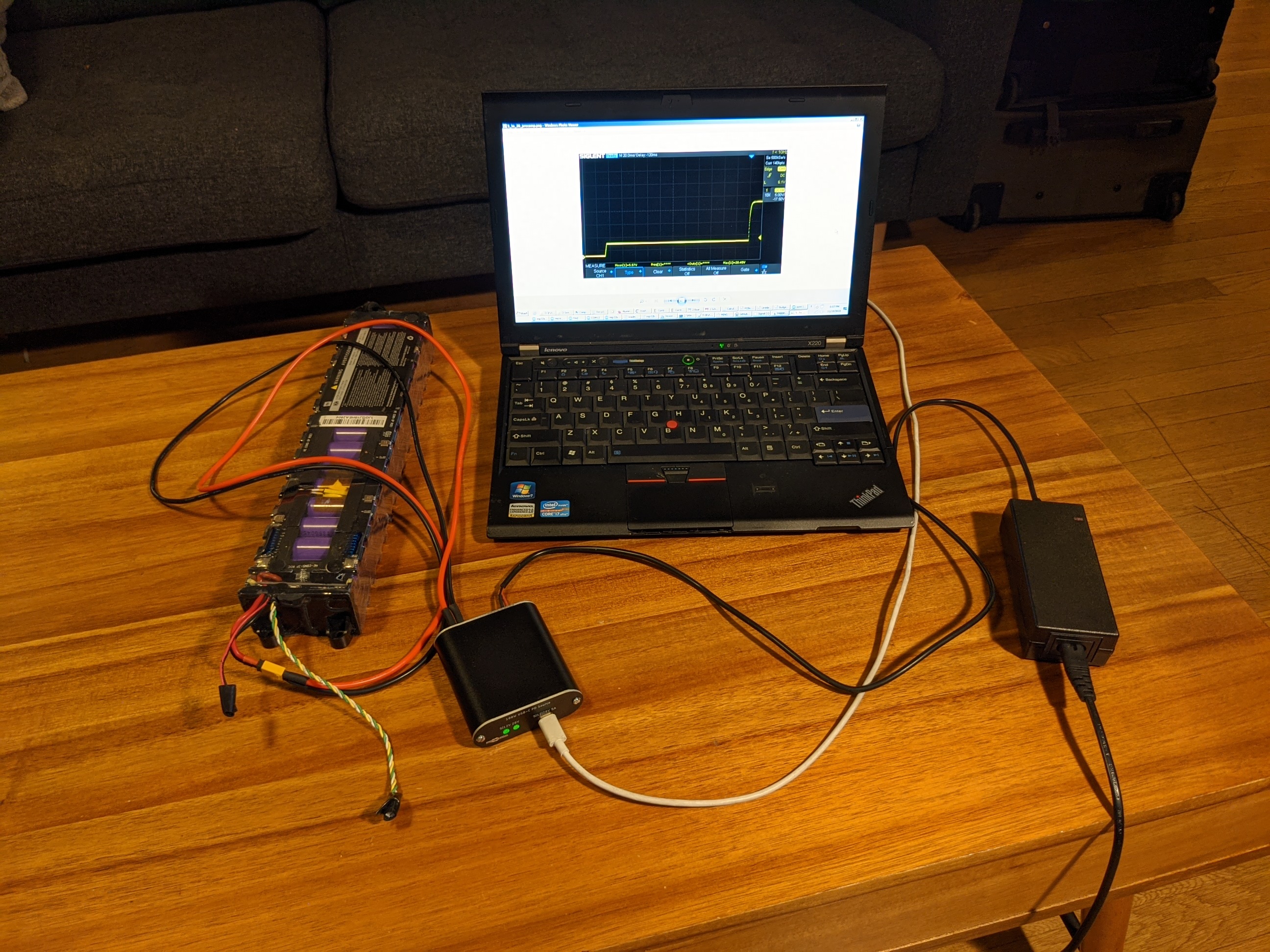
Thinkpad Running off of Charger with Scooter Battery
Background
USB-C PD (power delivery) sources advertise what voltage and power levels they are capable of using the CC (Charge Control) lines in USB-C cables. There are two CC lines -- which one is active depends on the orientation of the cable. Sinks then decide which of the available profiles they desire, and if it is something other than the default 5V the charger will ramp its output voltage up to match. New additions to the spec allow for up to 48V, but most existing products don't use anything higher than 20V. Most laptops use 20V and most phones will request 9V but will still fast charge at 5V if 9V is not available.
The CC protocol is supported by some microcontrollers, but there isn't a simple open source way of bit-banging it with an arbitrary microcontroller, so instead I used a dedicated charge controller IC. Some ICs of this sort are set up to work along with a microcontroller, but many support standalone operation since it wouldn't make sense to add an extra part to a cost optimized AC charger design. Texas Instruments TPS25740 is one such standalone part that was actually in stock when I designed this board. ST has its own part (STUSB4700) which I would have slightly preferred, but it was out of stock.
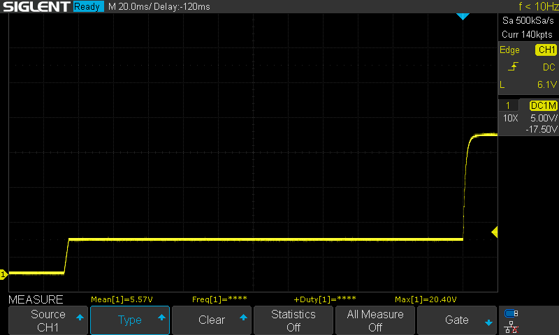
Output Voltage From Connection of PD Sink to 20V Output Transition
TPS25740 is configured by strapping resistors which limits the flexibility of what can be configured, but it makes for a dead-simple design. Some of these parts control output voltage by communicating with digital power supply controllers over PMBUS, but TPS25740 keeps things simple by adjusting the resistance to ground of the feedback node of the power supply in order to adjust the output voltage. For some reason, TI has marked this part NFND (not for new designs). While I do as good practice ordinarily respect NFRD warnings, this was the only part available at design time that met my requirements. I bought ten for possible future projects and called it a day.
Electrical Design
Buck Converter
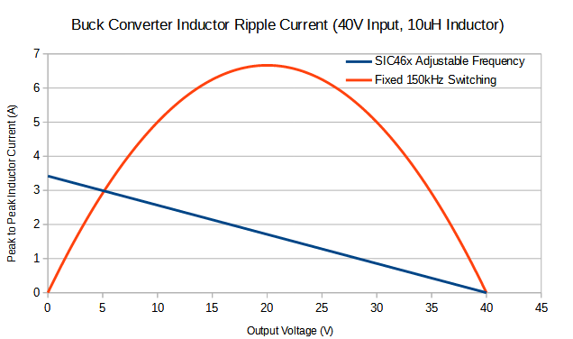
Supply of internal switch buck converters was also quite constrained when I designed this board, but new-to-market ICs are typically less constrained. Fortunately, Vishay had recently come out with a line of high current (10A) moderate voltage (60V) bus converter ICs that seemed ideal for this application. I chose the highest current option (SiC466) for flexibility. This controller has one unusual feature: the switching frequency is a function of output voltage. While it is not explicitly stated in the data sheet, this is a useful feature for adjustable output supplies.
With duty cycles below 50% in a buck converter, increasing duty cycle increases inductor ripple current. With SIC467, switching frequency is proportional to output voltage, so inductor ripple goes down with increasing duty cycle when input voltage is held constant. This means that the inductor will dissipate the most power (core + conduction losses) with a 5V, 5A output. Conversely, SiC466's internal losses are highest with a 20V 5A output (highest switching + conduction losses). Because inductor losses are highest at low output voltage and SIC467 losses are highest at high output voltage, the total losses varry less with output voltage.
Buck Converter Relative Ripple vs. Duty Cycle
I initially built the board with a 22uH inductor because I had optimized for 20% ripple current at 5V out, but the inductor was getting quite warm from ohmic losses at 20V out. I swapped it out for a 10uH inductor (which is the datasheet example) which kept losses at full load to a manageable level at the expense of slightly higher core losses. The switcher was also getting concerningly warm at full load, so I dropped the switching frequency by a factor of two to reduce switching losses at the expense of increased core losses. This guess and check methodology works pretty well for getting to a 90% optimal solution. You can analyze a problem to death to try to eek out the remaining gains, but your analysis is only as good as your models. Switching loss in an internal switch buck converter are hard to estimate, and inductor core loss models are unavailable from many manufacturers. If this were a commercial design, I'd test more frequency and inductor option, but, since this is a personal project, I'll call it good here.
Stability
I assembled two revisions of this board. I did not populate the 270uF aluminum polymer output cap on the first board, and it had great stability as shown in the gain-phase measurement setup picture later. I was using a cheap flash drive that decided to corrupt all of the screenshots from that testing, so what I have to show in detail is for the less stable board with a 270uF output cap. I populated this cap on the second board because I saw undesirable startup behavior with a USBC to Thinkpad Adapter: It works when plugging the USB-C side of the cable into the charger before plugging the Thinkpad end into the Thinkpad, but if the Thinkpad end is already mated when the USBC end was plugged in, the converter will over-current and get stuck in a loop. I though that additional bulk cap might help with this, but it did not. I think what is happening is that the Thinkpad adapter does not have a load switch to enable its output when 20V steady state is reached and instead passes its input directly to the Thinkpad. The Thinkpad then starts to draw current before the supply is at a stable 20V and the combined inrush of the internal charging circuitry turning on and the current needed to charge the caps during a voltage change trips the over-current.
Load Step Testing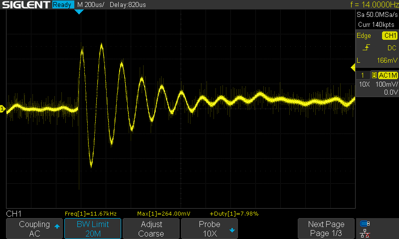
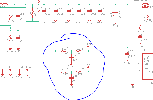
Load Step Transient Before Compensation Adjustment (270uF Al Output Cap)
The fastest way to get a sense of the stability of a power supply is stepped load testing. Here, I just manually plugged a load resistor into the output testpoint and measured the transient response. The immediate result was that the converter (I measured the board that I installed the aluminum polymer output cap on. The one without the extra bulk cap was actually fine) had pretty bad phase margin as indicated by excessive ringing. A general overview of load step testing can be found in this TI App note.
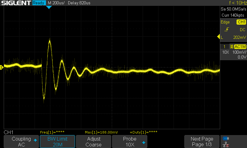
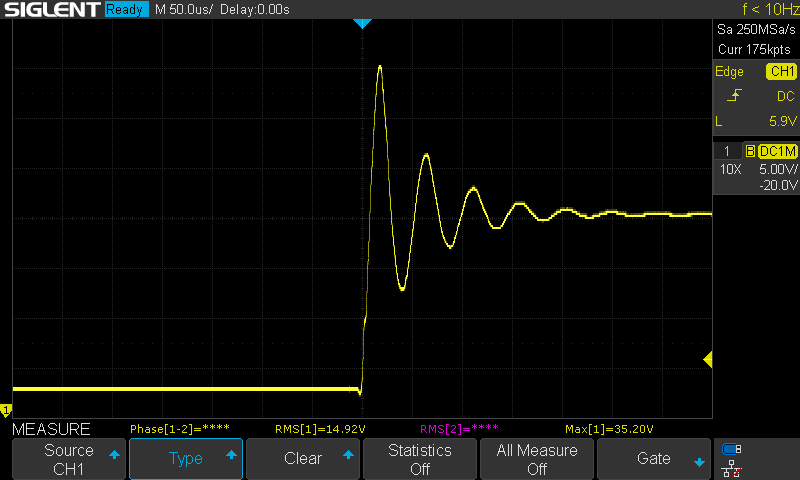
Load Step Transient After Compensation Adjustment (270uF Al Output Cap)
This is an internally compensated buck converter, so the only knobs that can be turned to adjust compensation are the output elements (inductor and capacitor) as well as feedback values and capacitive feed-forward. The datasheet does not mention adding feed-forward, and that is probably because excessive feed-forward values cause sub-harmonic oscillation of the converter (a short pulse followed by a longer pulse over and over instead of all pulses being of the same duty cycle). A small amount, 100pF, was enough to improve the phase margin to a point where I felt comfortable using this supply.
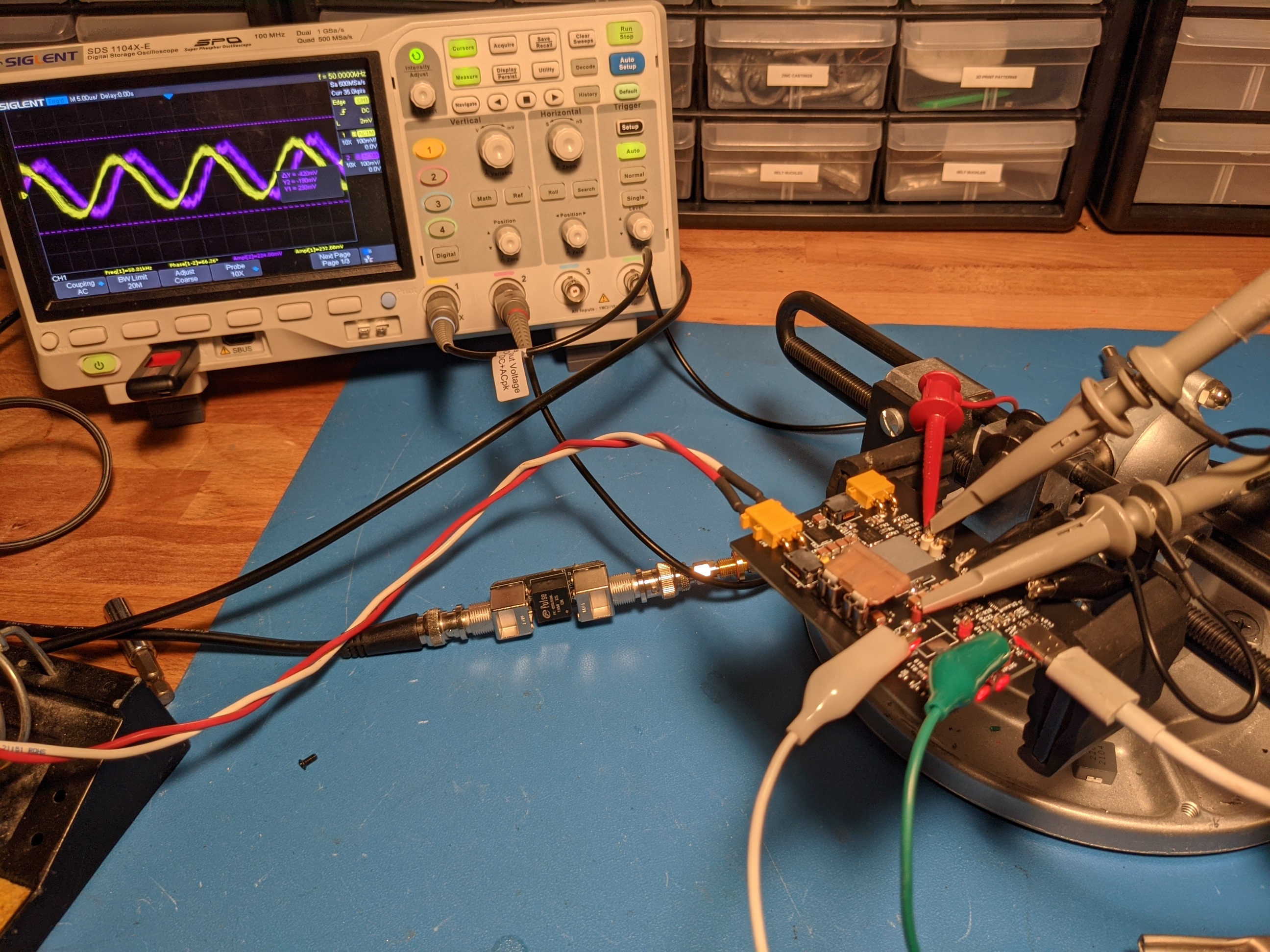
Loop Gain / Phase Measurement Setup showing 56° Phase Margin at a Cross-over Frequency of 50 kHz (No Al Output Cap)
Loop Gain-Phase MeasurementThe standard method of measuring the stability of analog power supplies is with gain-phase measurement. This can be done with just a function generator, a transformer, and an oscilloscope as long as you can add a small value (20 Ω) resistor at the top of the feedback divider to break the loop and inject a stimulus. The transformer is used to AC couple the stimulus from the function generator into the injection resistor — you can't generally connect the function generator directly because it would upset the DC level of the output of the converter and add noise due to ground potential differences. I use a pulse transformer for ADSL applications as an injection transformer. It has the widest bandwidth of any of a couple parts that I tried out and is quite inexpensive compared to parts sold for this purpose. At low frequencies, the transformer saturates and distort the injected signal and at high frequencies the parasitics fo the transformer attenuate the signal. Since gain-phase measurements are relative (based on two measurements on the board, not on the stimulus at the signal generator itself), it is easy to work around the limitations of crappy transformers in most cases.Instruments that use DSP to isolate the injected frequency from other noise (such as switching noise which can easily swamp an injected stimulus) are often used in industry for cleaner measurements. Here's a general overview of gain-phase testing: TI App note.
To measure phase margin, you connect one probe to the output of the buck converter and a second probe after the injection resistor (see the TI reference for more details). The loop gain at various frequencies can be measured by comparing the amplitude of the signal seen by both probes. When the gain is unity (i.e. at cross-over), the relative phase of the signals is equal to the phase margin. My scope's measurement of this lines up with what I would expect from the load step testing: 14 degrees before compensation and 22 degrees after compensation. Note that this isn't a particularly good result, and the obviously superior option is to just not install the 270uF output cap and accept the resulting 56° phase margin. A good rule of thumb for a general purpose power supply is to target a minimum of 45° of phase margin; 60° is close to a critically damped response, and the response becomes noticeably underdamped at 90°.
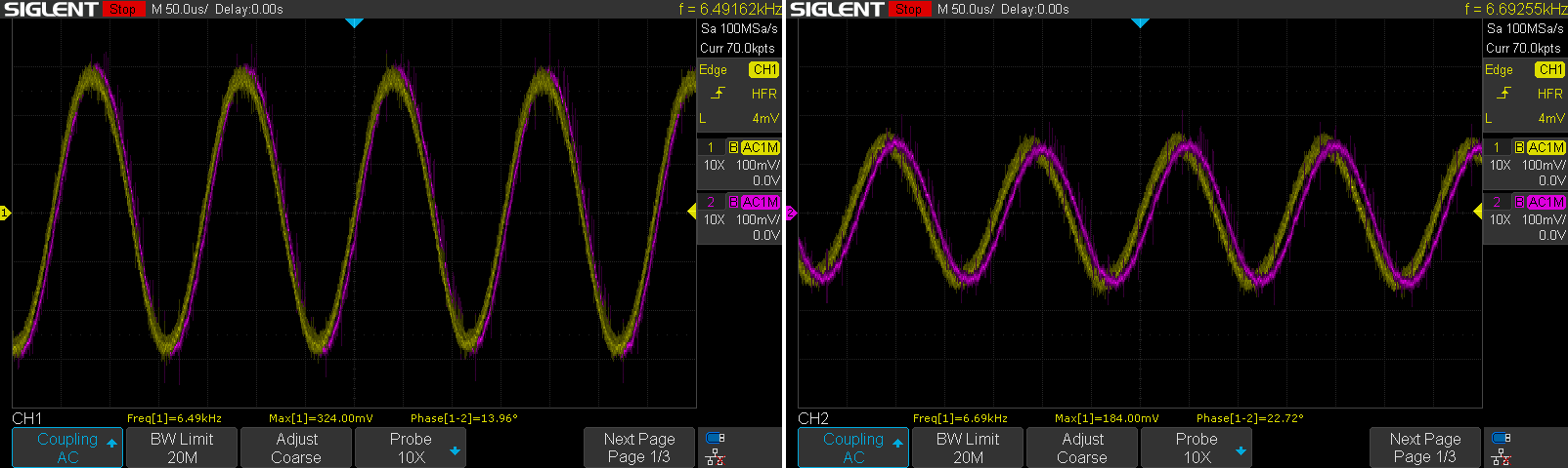
Phase Margin Before (left) and After (right) Compensation (270uF Al Output Cap)
Output Voltage Setting
TPS25740 can interface with any arbitrary supply because it is design to adjust the resistance from the feedback node of supplies to ground. This is accomplished by connecting two open drain outputs (CTL1 and CTL2) to the feedback node of the supply with different value resistors. With both CTL1 and CTL2 high impedance, the output voltage of the suppl is 5V. When CTL1 sinks current, the feedback divider is such that 12V is output and when both CTL1 and CTL2 sink, the divider is such that the output becomes 20V.
The USB-C PD Spec imposes maximum slew-rate requirements on VBUS when the sink requests higher voltages. For a 5V to 20V transition, the minimum transition time is 500 µs with a maximum slew rate at any point of 30mV/µs. Two options of implementing this are presented in the datasheet, (adding a much of transistors and adding balanced cap to the switched node), but I didn't like either of these options. Instead, I implemented something that I had need before in voltage margining circuits.
Slew Rate Limiting Circuit
Adding capacitance to the feedback node is generally no bueano because the resistance in the top half of the divider will form an RC filter with this added cap which will put a 90 degree phase delay into the sensed feedback above the cutoff frequency of this filter which is likely to destabilize the converter if its cross-over frequency is below or near the cutoff frequency of the filter. If, instead, this cap is added after a reasonable resistance, the cap can increase the slew rate without impacting the stability of the converter. As long as the soft start time of the converter is > the RC time constant of this hanger-on to the feedback node, it will not have a measurable impact on the operation of the converter when the opposite end (the end connected to the CTL lines) of it is high impedance. When that end is shorted to ground, the converter sees the resistors in parallel with its low side resistor which causes the DC output voltage to rise proportionally.
While this circuit does not appear in the datasheet for TPS25740 it does appear in whatever datasheet I sent Anton (Work Anton, not Gay Anton), so find that.
Input Filter
I added a common mode choke before the input filter to reduce conducted and radiated emissions. This may or may not have been necessary, but after seeing the horrible EMI put off by my power inverter which noticeably interfered with VHF narrowband radios, I decided to err on the side of over-designing the input filter on personal projects. The LC filter reduces conducted emissions at the switching frequency and first several harmonics of the switching frequency, and the ferrite bead helps knock down emissions at higher frequency, but I confess that I did not simulate it.
Worse-case underdamped ringing of an undamped input filter will result in a peak voltage twice that of the input (though I now wonder if it can actually be worse than that with ceramic capacitors which lose capacitance with increasing DC bias). If you hot-plug an undamped filter into a 40V supply, you will transiently see 80V at its output which, if you are using a 75V rated device, could destroy your power converter. To limit the peak voltage, you need to damp your input filter. I consider a "hot-plug" to be a connection of the charger to a zero impedance (infinitely stiff) source of a particular voltage. This is not a bad approximation for a large battery.
Input Filter Hotplug Transient into 20V Supply Prior to Damping
There are two main methods of damping and input filter: inductive damping (adding an inductor of lower inductance in parallel with the main filter inductor and putting it in series with a damping resistor) and capacitive damping (adding a higher value capacitor in parallel with your main filter capacitor and adding series resistance to it). Capacitive damping is commonly seen in commercial applications because aluminum capacitors intrinsically have significantly more series resistance than ceramic capacitors, so the parallel combination of ceramic and aluminum capacitors can make for a well damped filter without discrete damping resistors. Inductive damping sacrifices some of the filtering but has the benefit of not requiring a large value capacitor. Aluminum capacitors are often life limiting components in a design (they are expected to be the first to fail over time and temperature), so if you can design with no aluminum capacitors, you will have a design with a much longer expected life; this is why inductive damping is often seen on aerospace designs.
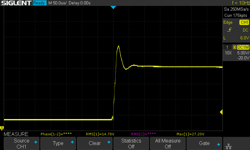
Input Filter Hotplug Transient into 20V Supply after adding 24.6 µF of Electrlolytic Capacitors
My input filter (which I lazily did not simulate) ended up being quite underdamped (peak voltage 1.75x input voltage), but this was not a problem with hot-plugs into a battery because the part is 75V rated and (with a maximum voltage of 42V on a 10S battery) the peak voltage would only be 73.5V. The problem is that the cheap Amazon 10S lithium-ion battery charger that I bought has a control loop so slow that it will overvolt the input if there isn't enough bulk cap. After adding 24.6 µF of electrolytic bulk cap, the filter was damped to where peak hot-plug voltage into a battery was only 1.35x input voltage and the peak hot-plug voltage with the crappy charger was only 56V.
Input Filter Hotplug Transient into El Cheapo Amazon Charger
I killed two SiC466 while determining what was wrong with the circuit which is annoying because the part was out of stock at this time. I had to settle for the lower current rated (6A) SIC467 on the final assembly, but that realistically isn't an issue.
USB-C PD Source Controller
USB-C PD Source controllers are hard to parametrically search for. Digikey does not properly separate source and sink controllers, so the results of a search are littered with inappropriate devices. Many source controllers are designed for microcontroller integration or for PMBUS power supplies. As far as I have found, TPS25740 and STUSB4700 are the only devices from 'reputable' manufacturers that can fill the role of a standalone USB-C source.
I strapped TPS25740 to support 5V, 12V and 20V outputs with 5A and 93W advertised. The rationale behind the 93W advertisement is that the controller wants to limit power drawn by the load to 100W even if the supply overshoots to 21.5V. If a device pulls 93/20=4.65A at 21.5V it will be drawing 21.5*4.65=99.98W. This is rather strange to me, though, because the limited power source requirements of IEC-62368 require that the load limit power itself, so telling the sink to limit its power draw doesn't let you omit over-current protection by the source. Over-current protection is still implemented at some margin above 5A by the source — this can be observed with commercial AC to USB-C adapters as well.
Since USB-C ports are by default bidirectional (can be either source of sink), they (unlike USB-A ports) do not by default apply power to the connector. Instead, they wait for a CC line to be pulled high by a slave device or for a PD-sink to communicate specific requirements over the CC lines. USB-C to USB-A OTG (on the go) adapters include the appropriate pull-up resistor to enable 5V outputs for legacy USB devices. Using such a USB-C OTG adapter, I can charge by 5V input Geiger counter.
Legacy Micro-USB Geiger Counter Charging off of USB-C Source with USB-C to Thinkpad Adapter in Foreground
Because USB-C ports are bidirectional, it is recommended/required that sources include back-to-back MOSFETs to make sure that current can neither feed out of or into the output port without the controller's blessing. The TPS25740 datasheet mentions that chargers with captive cables (male end only) do not need the extra MOSFET, so I did not implement one in my design despite by interface being a female USB-C. Even without this FET, I don't expect that plugging this charger into another charger would cause any issues because it doesn't ask for anything with its CC interface, and the default voltage of anything that it plugs into should be 5V. The body diode of the pass MOSFET would need to conduct for anything to make it from the output to the input, so as long as no more than 5V is supplied to the input, I don't expect that plugging this charger into another charger would cause any issues.
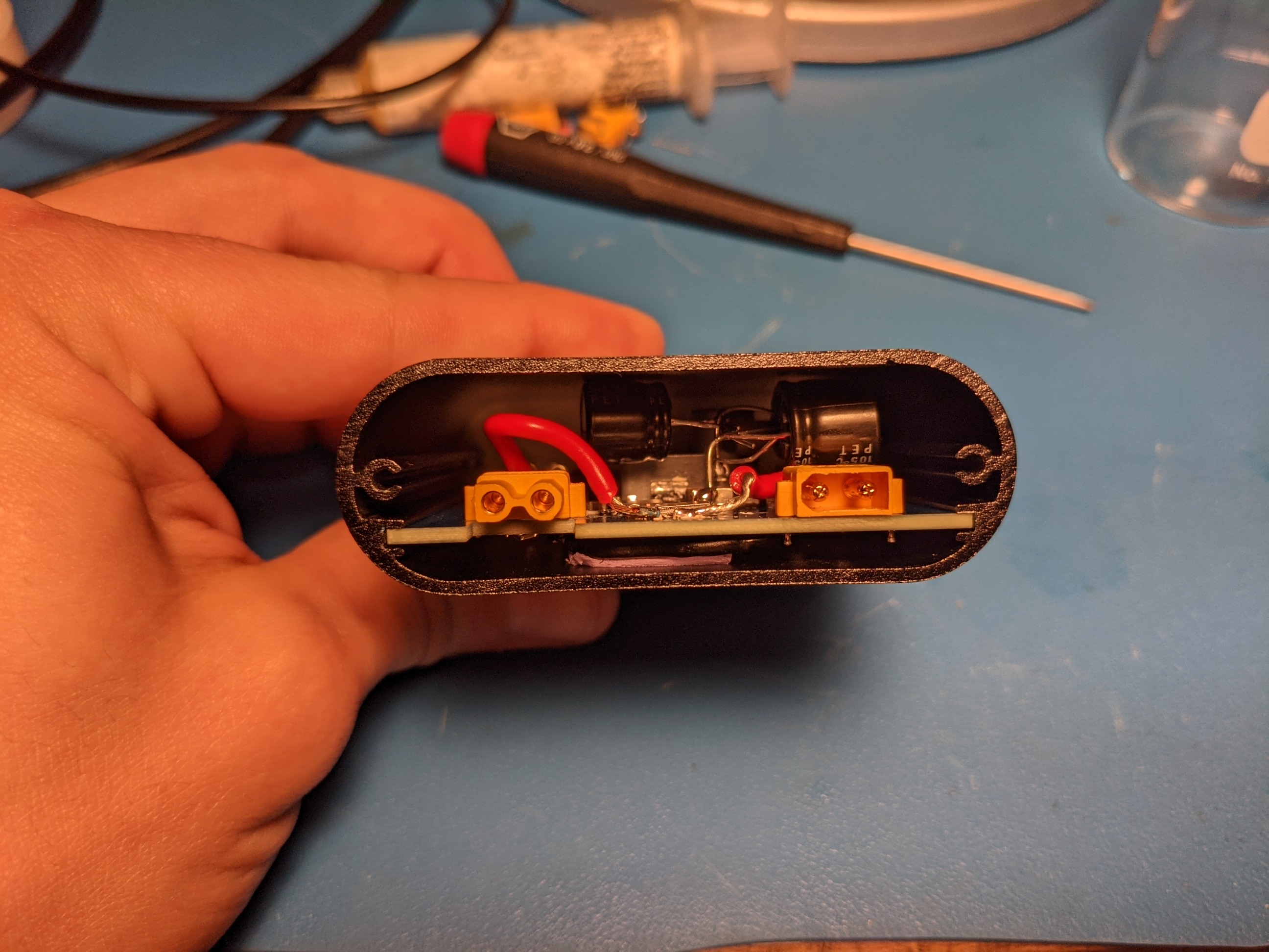
Mechanical Design
When building a one-off design like this, it is to your benefit to use an existing mechanical enclosure. I found an appropriately sized extruded aluminum enclosure on Amazon, bought several, and designed this board to them. The enclosure encludes card guides which allows the PCB to slot into the enclosure. By installing custom ends to the box, I can fix the PCB to one position with the connectors extending through the ends.
Bodged-on Aluminum Electrolytic Capacitors Inside Case
JLC PCB provides ridiculously cheap rates for prototype PCBs. They have recently added aluminum PCBs to their $2 for five special. These are boards that are composed of an aluminum sheet laminated to a single layer PCB. These have become quite popular for LED light fixtures where the aluminum board serves as a heatsink. I don't know if JLCPCB's $2 PCBs are just a loss leader or if they are an intentional program by the Chinese Communist Party to entice westerners into sending them designs with an economic or intelligence exploitation potential, but I'll take it if that means that I can get five aluminum PCBs for $2.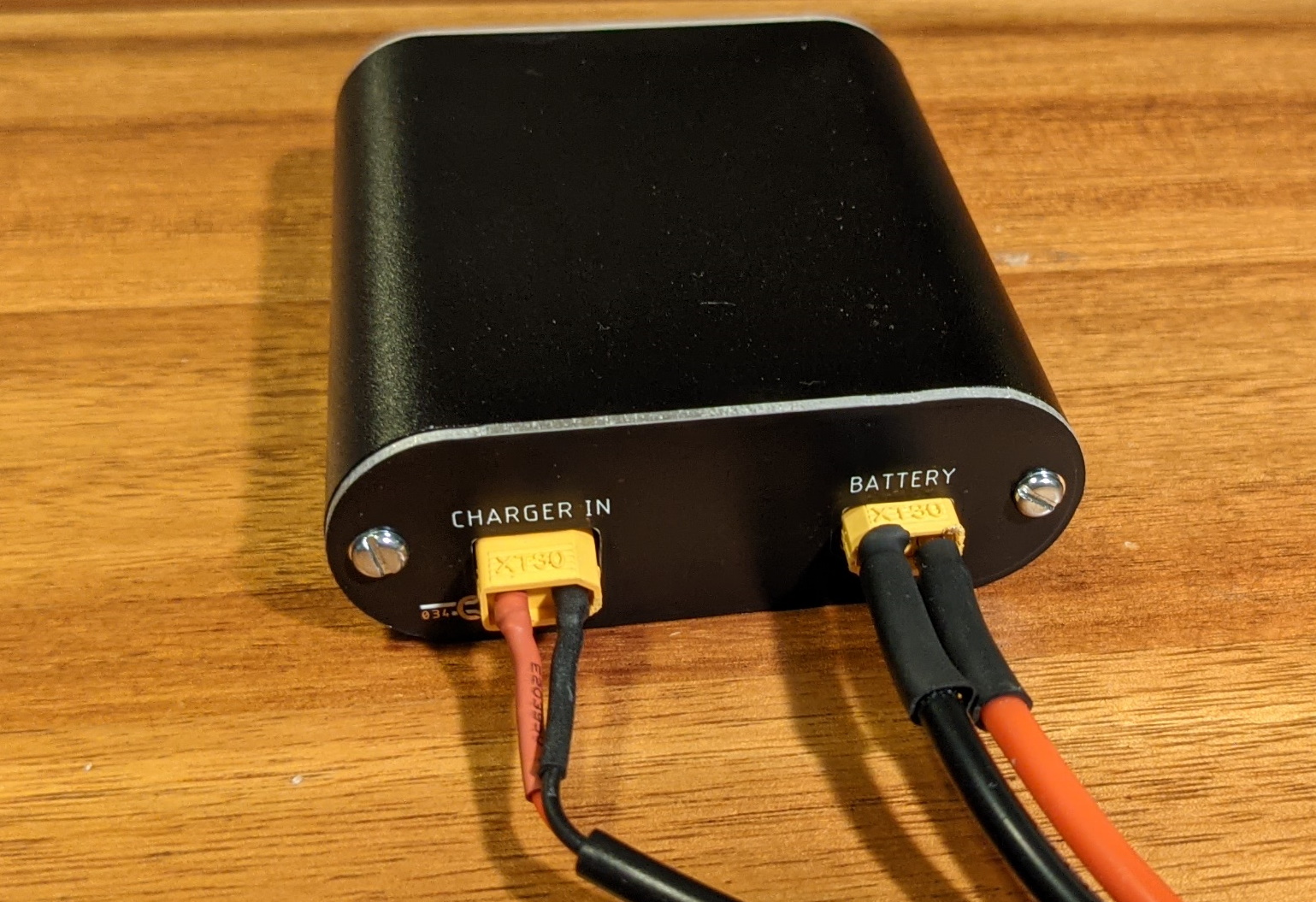
Black Aluminum PCB Back Panel
I've previously used ordinary 1.6mm FR4 circuit boards as the end of custom boxes, but having them be custom routed solid aluminum instead is a nice touch. I tend to make a lot of mistakes when designing the ends for boxes like this, so my design process is to 3D print an equivalent end and only order the PCB after confirming that the 3D print fits. After a few iterations, I had panels that worked for both ends.
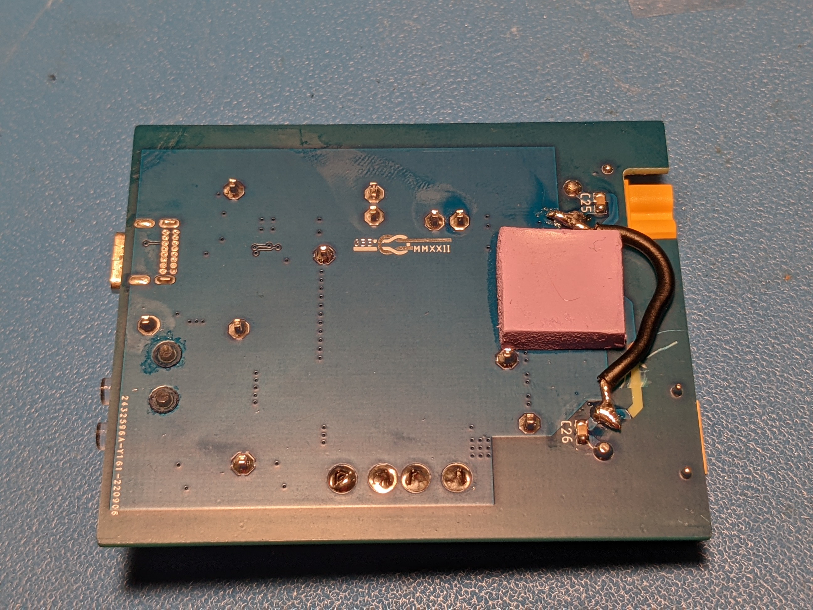
Location of Thermal Interface Material Pad
With a 100W output, the buck converter will overheat without a thermal path beyond the PCB itself. I added a silicone putty/rubber thermal interface pad under the converter to thermally bridge it to the case. Since the board needs to slide into the enclosure, it is necessary to compress the thermal pad a bit so that it does not get sheared off. After getting the PCB into its final location, I shoved the sides of the thermal pad in so that it made good contact with both the PCB and the case. After doing this, the supplies works reliably with any load, but this is definitely not a good design for mass manufacturing.
Revisions
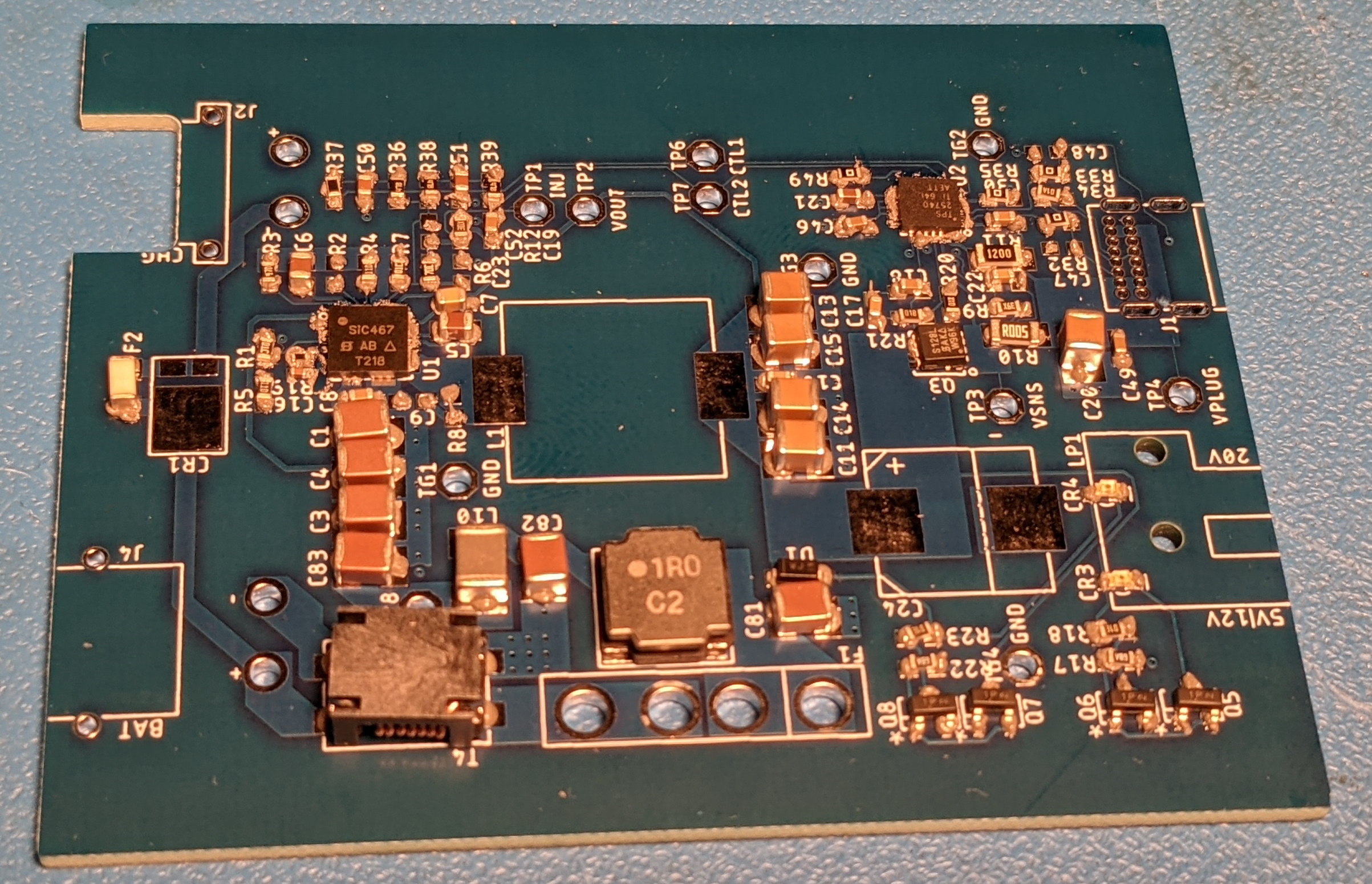
Revision 1 (Black PCB)
I made two revisions of this board, but a third is in order if I build any more. There were two issues with the first revision: The footprint of the charger connector was incorrect and the symbol for the USB-C connector connected CC2 to the wrong pin and as a result the charger only worked when the cable was inserted in one orientation. I was specifically incentivized to fix the latter problem after a friend with a phone with a damaged USB-C jack was not able to charge off of my converter because it was broken in the opposite way with respect to CC lines! The second revision fixed both of these issues, but I accidentally wired the charger connector backwards, and I also determined at this point that the input filter required additional damping. I've been using the revision two board daily to charge my cell phone, and I also use it to charge my Thinkpad X220 when I am out and about, so I'll only design a third revision if I have reason to build additional boards.
Revision 2 (Blue PCB) Prior to Reflow
Many things that were designed before the advent of USB-C have now been adapted to USB-C. I use a USB-C to Thinkpad adapter which seems to signal only that the laptop desires 20V and does not include a power switch to enforce that the Thinkpad wait for the voltage to stabilize prior to drawing power. Neither revision of the board (with or without the aluminum output capacitor) was able to power the Thinkpad when plugged into the Thinkpad first and USB-C second. An off-the-shelf 100W USB-C AC adapter also had trouble with this particular adapter and eventually failed after repeated use. So I believe the situation is that the aftermarket adapter is grossly out of spec and that my charger's sequencing requirements are a result of the adapter being bad rather than my charger being bad.
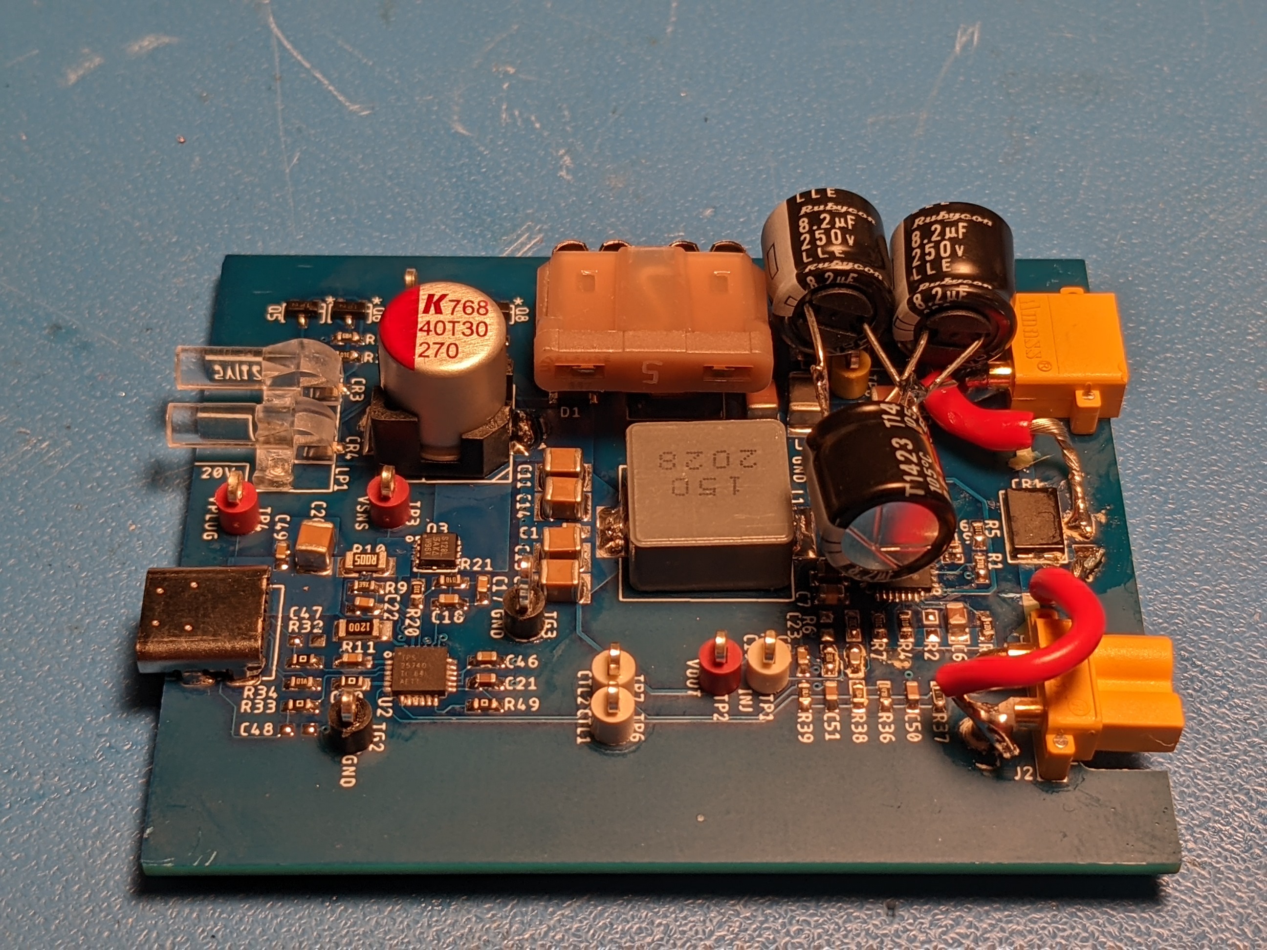
Revision 2 After Reflow and THT Assembly. Red Wires Correct for Charge Port Polarity Swap
One other less than DFM friendly modification was bending the input fuse 90 degrees to fit inside the case. These automotive fuses and fuse holders are cheap, but they are often only rated to 36V and take a fair bit of vertical clearance, so they aren't really the best pick for this project.