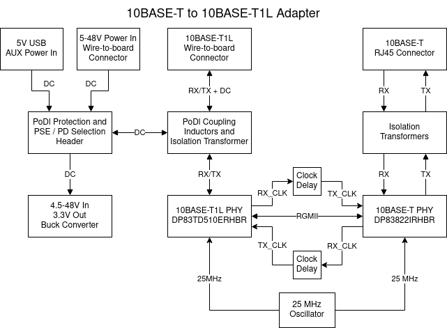
10BASE-T to 10BASE-T1L Adapter
2024
Project GitHub RepositoryTraditional copper Ethernet is limited to 100m or so and requires at least two differential pairs. In the past, if you wanted to run Ethernet over a longer copper cable, you would need to use a finicky, often proprietary and expensive Ethernet to DSL adapter. 10BASE-T1L applies the link training, equalization, and echo cancellation techniques used in more recent full duplex standards like 1000BASE-T to enable full duplex 10 Mbps communication over a single twisted pair with link lengths over 2 km.
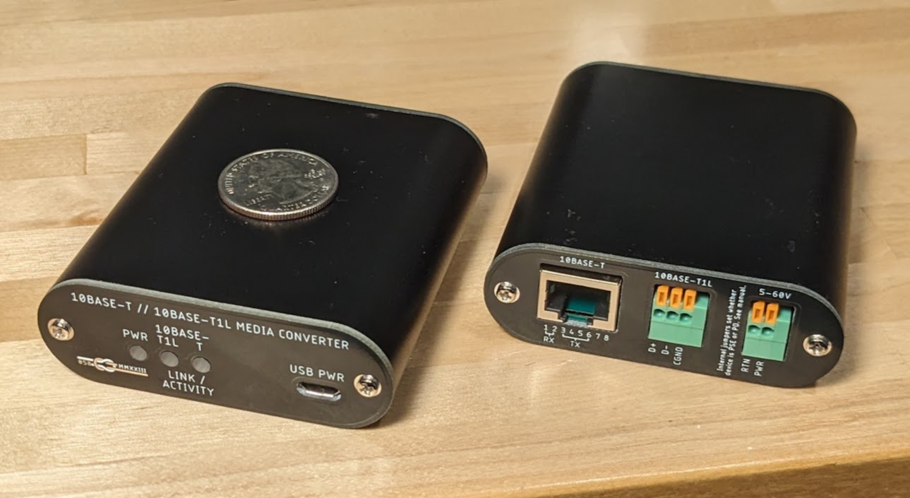
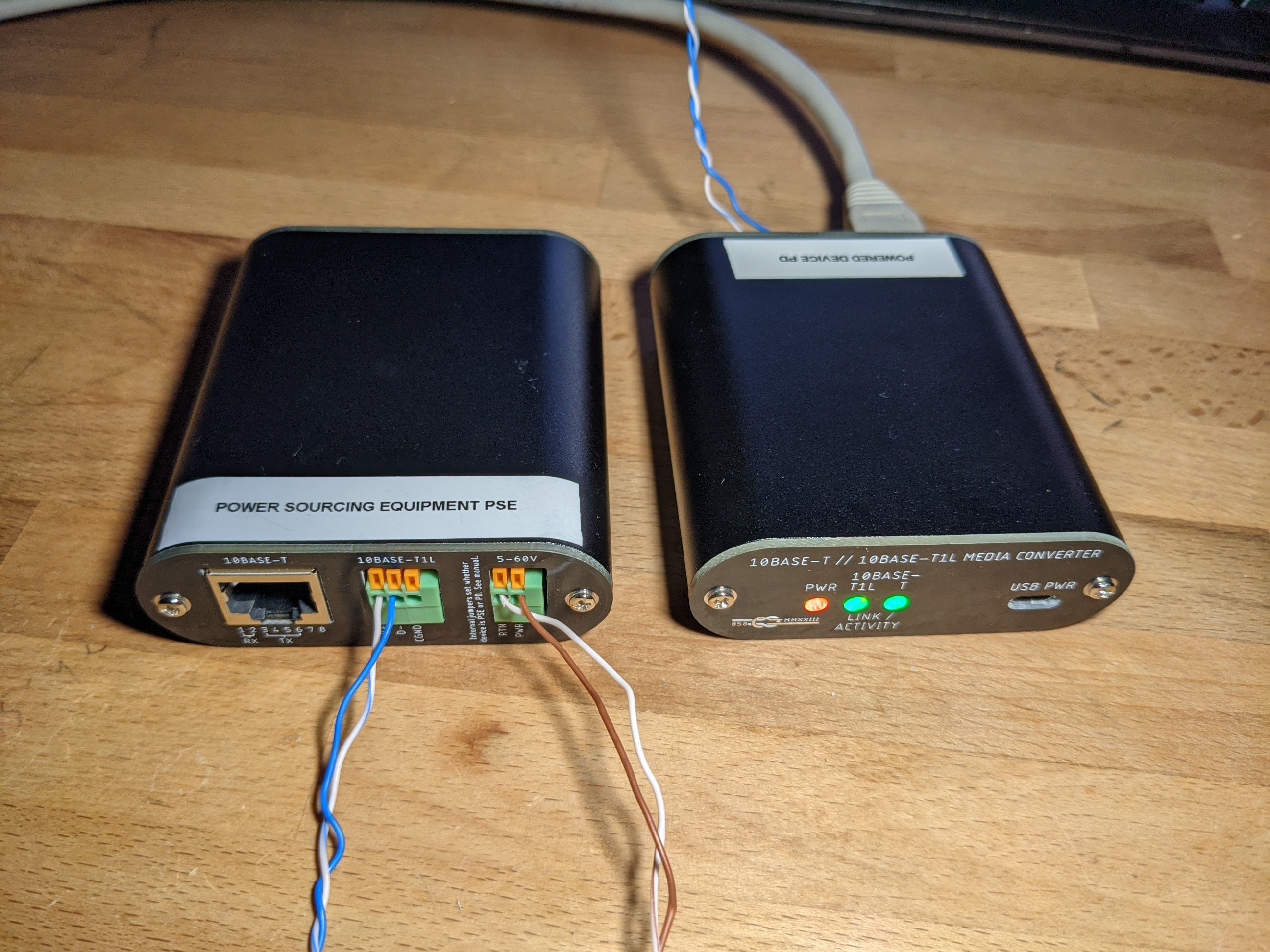
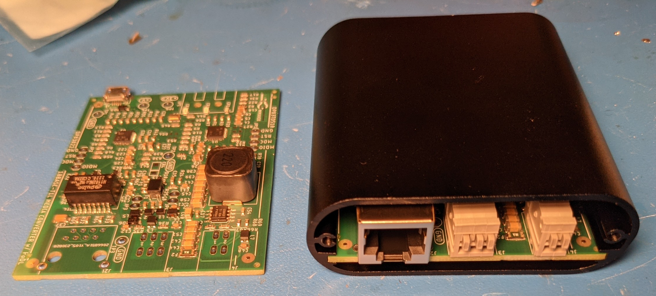
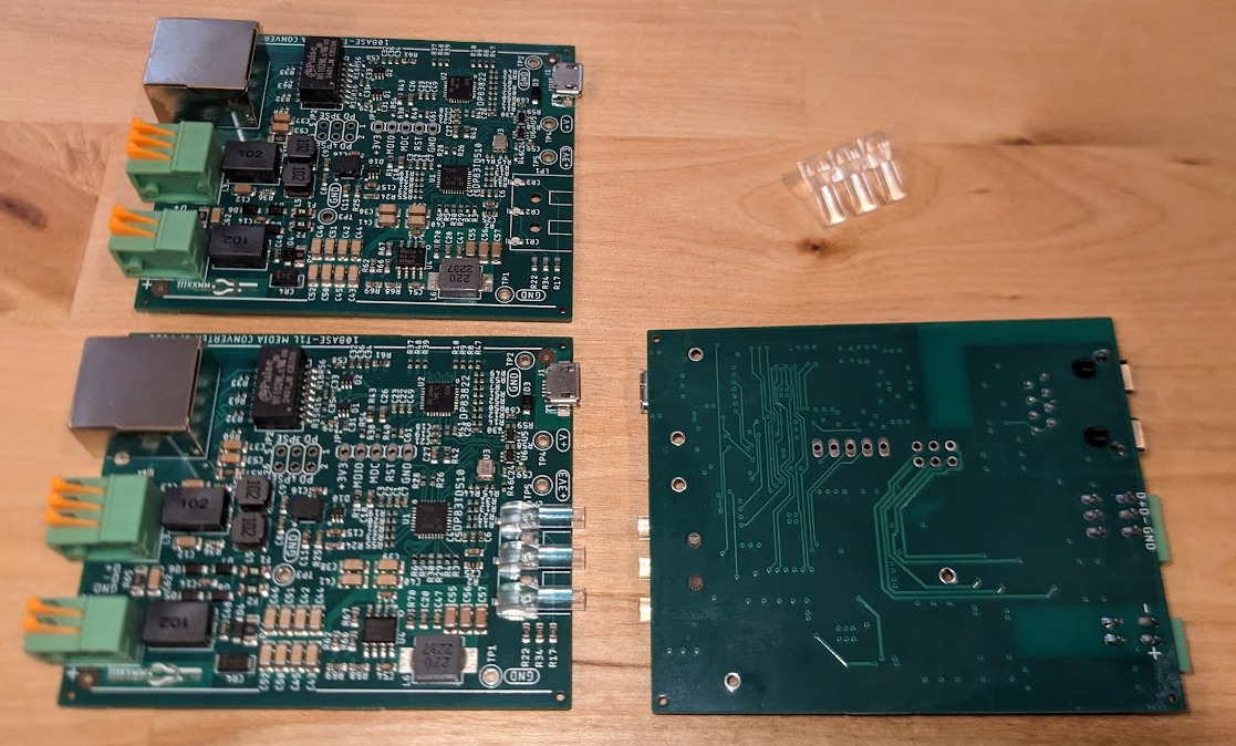
Completed 10BASE-T1L Adapters
There were no open source 10BASE-T to 10BASE-T1L media converter designs that I could find when I started this project. The aim is simple: build a 10BASE-T1L media converter with a nice enclosure which supports one end being powered with PoDL (Power over Data Line). For just media converters, having one end powered over the line isn't terribly useful since there is going to be something else at the remote end that the converter plugs into with 10BASE-T that will also need to be powered. I included the circuitry anyway so that I could learn about it for future use. When supplied by 48V at one end, you can pull ~3W from the remote end through 3000' of 23 AWG CAT-6 cable which is plenty enough to run a microcontroller with a camera and sensors.
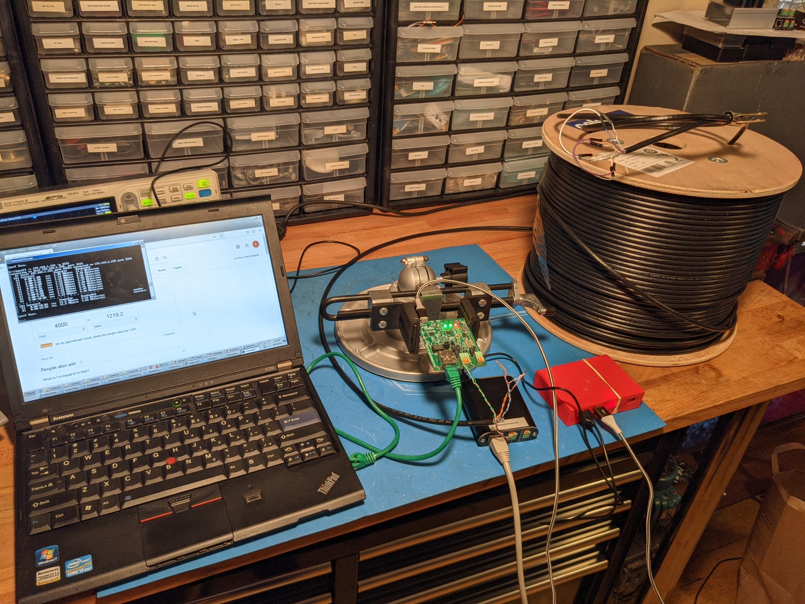
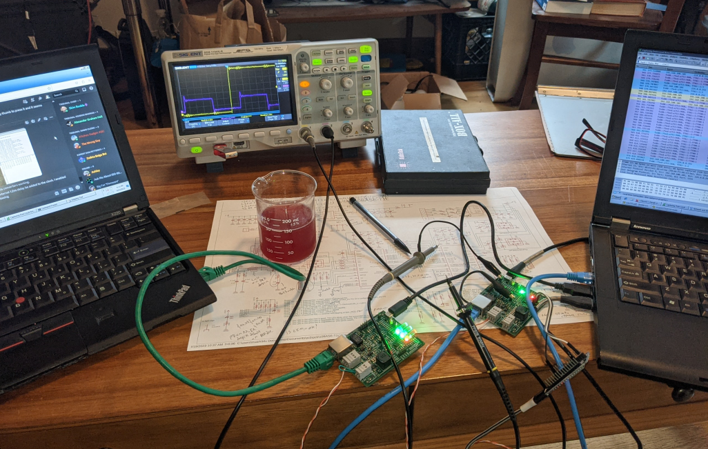
Testing performance through 4000' of CAT-6 Cable
The final design exceeded link length expectations: per the maximum link attenuation profile provided by the IEEE spec for 10BASE-T1L (802.3cg), I expected the link to break after about 2000 ft. of CAT-6 Ethernet Cable. In practice, the link comes up immediately with zero packet errors through 3000' (0.91 km) of CAT-6 and has trouble with link training at 4000' (1.22 km). When it does get through link training at 4000' (which TI documentation suggests can be helped by disabling auto-negotiation), the link stays up indefinitely and appears to be error free.
I went in pretty deep detail describing how 10BASE-T1L works, so if you are only interested in the design and implementation of this adapter, skip down to "Design."
How 10BASE-T1L Works
10BASE-T1L allows for bidirectional (full duplex) transfer of data at up to 10 Mbps using a single pair of wires. At first it sounds a bit like magic to simultaneously receive and transmit data using a single pair of wires, but this is exactly what analog telephones do using hybrids. Basically, If your transmitter has non-zero output impedance, then the voltage at the line will be an impedance divided ratio of the local transmitter's output and the remote transmitter's output. The signal from the remote transmitter will be attenuated with longer cables so in reality it is a bit more complicated since I haven't implemented equalization and echo cancellation, but here's a working toy model:
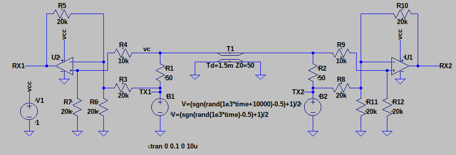
Full Duplex Transmitter Model
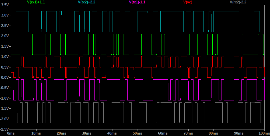
The RX signals are produced by adding the local TX signal by -0.5 to the voltage on the line and then multiplying that sum by 2. The simulation shows that you can easily recover the remote signal using this method:
Extracting Received Signals from Shared Full Duplex Line with Knowledge of Transmitted Signals
The received signals exactly match the transmitted signals with a 1.5ms delay due to the transmission line. Note the output resistance of the transmitters: 50Ω. This value was chosen to match to the 50Ω transmission line. In 10BASE-T1L, the line is a 100Ω differential pair which you can treat as two separate 50Ω single ended lines. If the impedance of the line does not match the impedance of the terminations, you get reflections which will distort the signal. Here is what happens when you change to a 300Ω transmission line without adjusting the termination impedance:
Distortion on Received Signals due to mismatched (300Ω) Transmission Line
Twisted pair wire is used for Ethernet instead of single ended coaxial cable because it is cheaper and easier to terminate. You could run 10BASE-T1L over a 50Ω cable if you used appropriate baluns at each end which would let you relive the ignominious days of 10BASE5. You won't have multidrop support, but you will have a range of 2 km based on attenuation at 10 MHz in typical RG-8/U cable.
Unlike in my toy model, 10BASE-T1L encodes data using a three level (PAM3) modulation. Specifically, the four RGMII received bits are scrambled and then encoded into three ternary symbols (4B3T) which ensures that no DC bias accumulates on the line. There are 16 possible 4-bit words and 27 possible 3-trit words which allows multiple 3-trit codewords to map to individual 4-bit words which allows options for maintaining DC balance as shown here:
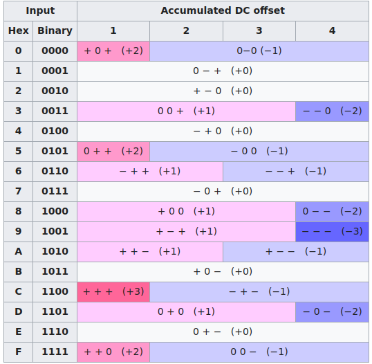
4B3T 4-bit to 3-trit Codeword Mappings
DC balance is required for any signal that is to be coupled through a transformer. 10BASE-T avoids DC bias with differential Manchester encoding, and 100BASE-TX uses MLT-3 encoding. While 4B3T encoding ensures DC balance, scrambling of the data in 10BASE-T1L ensures that there are sufficient transitions to easily clock the received data and that the power spectral density of the data is spread out to reduce unintentional radiated emissions. Since there are 4/3 bits per symbol, the line rate of 10BASE-T1L is 3/4*10M=7.5 MBd.
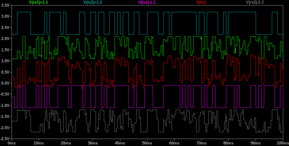
Superposition of RX and TX Signals with 10BASE-T1L: Pink = TX_P Pin. Yellow = Line_P.
The above plot shows the output of a PHY (pink) and the line voltage which is the average of the local PHY and the remote PHY TX voltages. As a result, there are three levels in the PAM-3 output of one PHY before the 50R termination resistor and five levels present on the line [(-,-);(-,0)|(0,-);(0,0);(0,+)|(+,0);(+,+)]. As with my toy LTSPICE model, you can subtract half of the local transmit signal (note that I have set it to half the scale of the line voltage) and from that determine the transmit PAM-3 signal of the remote PHY.
Auto-negotiation
Before actually running data, the PHYs need to know a couple things about their link partner. This is accomplished using auto-negotiation. The two main parameters that need to be configured are which PHY acts as the Master and what voltage level is to be used. In 10BASE-T1L, the master PHY clocks its output from its local clock, and the slave clocks its output from the the recovered clock. Which PHY acts as the master and which acts as the slave is determined randomly with auto-negotiated links. For voltage, there are two transmit levels allowed by 10BASE-T1L: 1.0 Vpp and 2.4 Vpp. If both PHYs support 2.4V, then that is used. Otherwise, 1.0 Vpp is used. There are a few other special capabilities like energy efficient Ethernet that defines ways of muting data transmission when there is no link activity and whether a link is 10BASE-T1L or 10BASE-T1S. This is all defined in tables 45-330A and 45-330B in IEEE 802.3cg.
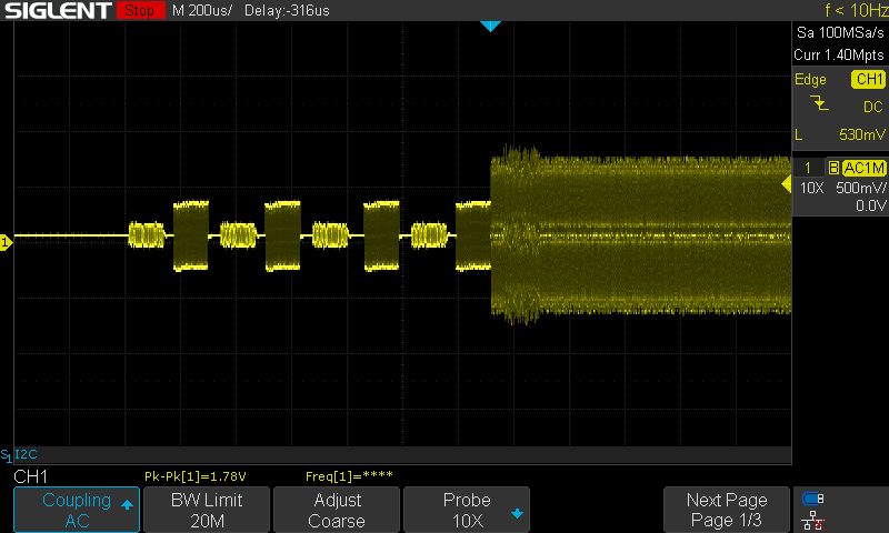
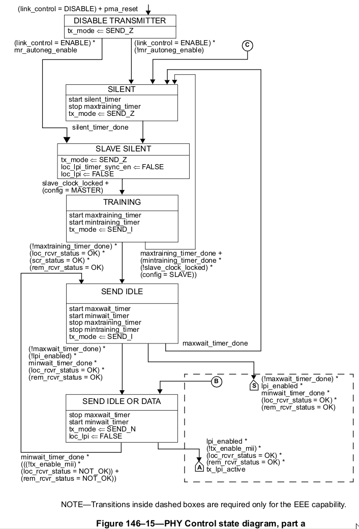
Four Remote LSM Auto-negotiation Frames and Four Local Frames (Note Amplitude Difference) Followed By Link Training over a 3000' CAT-6 Cable
Auto-negotiation in 10BASE-T1L by default operates using half-duplex Differential Manchester Encoding (DME) at 625 kb/s. This is referred to as Low Speed Mode (LSM). All other single pair Ethernet standards (10BASE-T1S, 100BASE-T1, 1000BASE-T1) auto-negotiate by default using High Speed Mode (HSM) which is DME at 16.667 Mb/s. A PHY with nothing connected to it will send auto-negotiation messages periodically until a remote phy responds with auto-negotiation messages of its own. Autonegotiation is half-duplex, so each PHY will send its message and wait for an appropriate reply before either timing out or sending a subsequent message.
Unlike with 10/100/1000BASE-T Mbps Ethernet, I am not aware of any single pair Ethernet PHYs that are able to auto-negotiate between different line rates. If you buy a 100BASE-T1 PHY, it is not going to support 10BASE-T1S. From the standards it seems like it would be possible to build such a PHY, its just that no one has done so yet. You also can't connect a 10BASE-T1S PHY to a 10BASE-T1L phy because they encode data entirely differently. 10BASE-T1S sends 4B5B encoded data using differential Manchester Encoding at 12.5 MBd while 10BASE-T1L as previously mentioned sends 4B3T encoded data using PAM3 at 7.5 Mbd.
Link Training
Link Establishment State Diagram from IEEE 802.3cg Section 146.4.4.3
After auto-negotiation completes, the PHYs begin sending data that allows them to tune their echo cancellation and equalization circuits. IEEE 802.3cg does not define exactly how receivers need to implement echo cancellation and equalization. In fact, it only says "To achieve the indicated performance, it is highly recommended that PMA Receive includes the functions of signal equalization and echo cancellation." I think this is why the TI DP83TD510 PHY (which I used in this project) is able to achieve 2km long links when appropriate wire is used: TI put good equalizers into the part and achieved much better than the minimum level of performance specified in the standard.
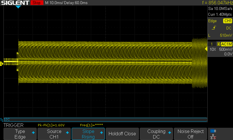
Link Training where the Local PHY is the Master
link training in 10BASE-T1L is accomplished just with idle messages (SEND_I): "During training operation (when tx_mode is SEND_I), knowledge of the transmitted symbols may be used at the receiver side to perform any signal conditioning necessary for meeting the required performance during normal operation. When the link is up, the PHY enters SEND_N mode and the transmitted PAM3 symbols are used at the receiver PHY for continued clock frequency/phase tracking." It seems that the PHY acting as master immediately begins sending idle symbols after auto-negotiation completes, and the phy acting as the slave mutes its output (SEND_Z state which sends 000 symbols) until it locks its clock to the master PHY's clock. Both the master and slave then send idle messages until both PHYs show that their de-scramblers are synchronized and that the link is good. The remote phy communicates that its link is good by encoding "loc_rcvr_status" with its scrambler function as defined in IEEE 802.3cg section 146.3.3.4.3. Once both ends are happy with the link, the PHYs will send data (SEND_N) if there is any to send and will otherwise continue to send idle sequences.
Link Training where the Local PHY is the Slave (Line Data is from Remote Master when Local Slave is SEND_Z State)
Maximum Link Length
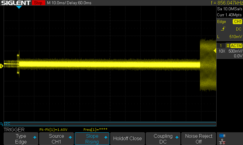
The maximum link length for 10BASE-T1L is defined by the maximum allowable attenuation. IEEE 802.3cg defines two attenuation limits (valid 0.1-20 MHz) depending on the operating amplitude:
\[IL_{1.0Vpp}(f) \le 5.9 \left( 1.23\sqrt{f}+0.01f+\frac{0.2}{\sqrt{f}} \right) + 0.2\sqrt{f} \text{ (dB)} \tag{1}\] \[IL_{2.4Vpp}(f) \le 10 \left( 1.23\sqrt{f}+0.01f+\frac{0.2}{\sqrt{f}} \right) + 0.2\sqrt{f} \text{ (dB)} \tag{2}\]This implies a maximum attenuation of 10.3 dB at 100kHz, 25.6 dB at 3.75 MHz, and 58.3 dB at 20 MHz for 2.4 Vpp operation. The trailing \(+ 0.2\sqrt{f}\) term accounts for the impact of ten in-line connectors. The TIA-EIA-568-B standard for twisted pair cable defines the maximum insertion loss of Category 5e cable as:
\[IL_{cable,100m}(f) \le 1.967\sqrt{f}+0.023f+\frac{0.05}{\sqrt{f}} \text{ (dB/100m)} \tag{3}\]This equation isn't terribly accurate at low frequencies, but that isn't the limiting factor here. The maximum in-spec cable length can be found by plotting the curves and adjusting the length of the cable so that there is margin to the two limits. The result is about 350 m for 1.0 Vpp amplitude and 600 m for 2.4 Vpp amplitude. This is a lot better than the 100 m limit for 10/100/100BASE-T, but it ain't 1 km. To achieve 1 km and remain in-spec, you need expensive industrial automation cable like Siemens 6XV1830-5EH10 which has a loss of 42 dB/km at 16 MHz which has margin to the 52.1 dB limit at that frequency defined by equation 2. Unfortunately, this cable costs $2879.76/km, so I will stick with CAT-6 for my own experiments.
10BASE-T1L Maximum Insertion Loss
In reality, good quality ethernet cable will beat this spec with decent margin, so the actual supported link length will be greater than what the maximum insertion loss limits suggests. Similarly, the maximum insertion loss limits are well, you know, just like IEEE's opinion, man. There is no physics based reason why the maximum supported attenuation is 25.6 dB at 3.75 MHz. The power spectral density limit for 2.4 Vpp transmit amplitude is -56 dBm/Hz at 3.75 MHz while the thermal noise floor is -174 dBm/Hz. After insertion loss of 25.6 dB, the receiver would see -82 dBm/Hz which is 92 dB above the noise floor. I chose 3.75 MHz for this calculation because it is the fundamental frequency of a 7.5 Mbd signal: If you send +-+-+-+- at 7.5 Mbd, the square wave you get on the line has a frequency of 3.75 MHz.
An actual calculation of bit error rate requires the full bandwidth of the signal to be considered which is complicated by the PSD of the signal varying over frequency, but with a lot of hand-waving and approximating the bandwidth efficiency of PAM-3 to be 1 bps/Hz, you can compare the theoretical eb/No to this SNR value and see that a real-world system could work with far more attenuation.
Using equation 5-2-46 from the third edition of Digital Communications by John Proakis, the probability of error for M-ary PAM is:
\[BER = \frac{2(M-1)}{M}Q\left( \sqrt{\frac{(6log_2M)e_b}{(M^2-1)N_o}}\right) \tag{4}\]For PAM-3, this becomes:
\[BER = \frac{4}{3}Q\left( \sqrt{\frac{9.51e_b}{8N_o}}\right) \tag{5}\]Which results in a BER of ~1e-11 at an eb/No of 16 dB. Again, this is very sloppy analysis, but decibels are forgiving. Adding another 10dB of margin to this, you can safely say that a real-world system could operate with 2x the (dB) attenuation specified for 10BASE-T1L if there are no other sources of noise, if the receiver has a low noise figure, and if the line equalization circuitry is well designed. In practice, designing a commodity ethernet device to achieve noise-limited performance is not going to be economical which is why IEEE specified a more conservative insertion loss limit. That doesn't, however, stop the manufacturers of PHYs from building chips that beat the standards-defined limit.
Note that the the IEEE spec specifies that the receiver can tolerate -106 dBm/Hz gaussian noise with a 10 MHz bandwidth while maintaining a BER below 1e-9. In a system with this level of noise present, no improvement in receiver design would be able to extend links much beyond the specified maximum attenuation value. The back of the envelope -82 dBm/Hz number I listed earlier has 24 dB of margin to this noise value. In reality, there is more signal energy at lower frequencies where attenuation is lower which results in a higher SNR in practice. Will having multiple 10BASE-T1L links in the same CAT-5e cable cause interference? I am no expert in cross-talk calculations, but it seems like the limiting factor here is going to be near-end cross-talk since any far-end cross-talk will be attenuated by the insertion loss of the cable significantly. With a -56 dBm/Hz PSD at 3.75 MHz and a 100 m section of CAT-5e cable having a Power Sum Near-end Crosstalk (PSNEXT: sum of NEXT from the three other pairs in a 4-pair cable) of -53.3 dB at 4 MHz, the expected interferer signal is going to be something like -109 dBm/Hz. My best guess at how to calculate this for longer link segments is to sum the impact 100 m at a time. If I assume a system with ten 100 m links each with -53 dB NEXT which are summed, the total would be 10log(10)-53 dB=-43 dB. However, this ignores attenuation in each segment. With 4 dB/100m attenuation at 4 MHz, each subsequent 100m section contributes 8 dB less to NEXT since both the interferer and the cross-talk are attenuated by 4dB as they travel through the cable:
\[NEXT_{1km} = 10log_{10}\left(\sum_{i=0}^9 10^{\left(\frac{NEXT_{100m}-8i}{10}\right)}\right) = 10log_{10}\left(\sum_{i=0}^9 10^{\left(\frac{-53.3-8i}{10}\right)}\right) = -52.6 \text{ (dB)} \tag{6}\]This would suggest that at high frequencies, NEXT approaches a maximum value within the first 200m of the cable and does not appreciably increase beyond that. With a PSD maximum of -54 dBm/Hz at any frequency, it seems that near-end crosstalk from three other 10BASE-T1L link segments in the same cable would be no more than -106.6 dBm/Hz which is (possibly coincidentally) within 1 dB of the interferer power level defined in the spec! So, if you're using CAT-5e cable, you can reliably run four 10BASE-T1L links in the same cable as long as you don't greatly exceed the insertion loss requirements.
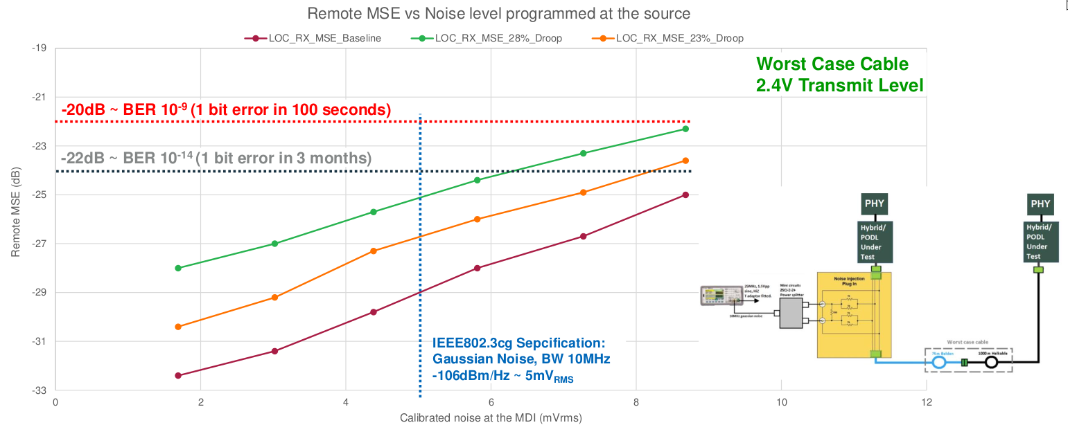
Analog Devices MSE vs. BER
This slide from an Analog Devices presentation where they argued for increasing the allowable droop (which I will cover in the next section) in 10BASE-T1L shows the impact of noise on error rate. They show an MSE (MSE = Mean Squared Error which is SNR but accounts for interference in addition to noise) of 29 dB with a -106 dBm/Hz interferer which implies a received signal with an average power of -77 dBm/Hz which is 5 dB higher than my back-of-the-envelope number which makes sense due to the lower attenuation of signal power at lower frequencies. The phrasing "remote MSE vs. Noise level programmed at the source" is a bit ambiguous about whether MSE is for the end where the noise is being injected or the far end where that noise would be greatly attenuated by the cable. IEEE 802.3cg makes the setup clear:
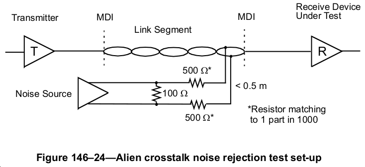
Alien Crosstalk Noise Rejection Test Set-up From IEEE 802.3cg
The other interesting thing about the graph from Analog Devices is that it shows (though it may be mislabeled since the -20 dB marker is lined up with -22dB MSE) that a 1e-9 BER requires a -20 dB MSE. This is within 4 dB of my value I estimated for a BER of 1e-11 and shows the utility of bounding results based on theoretical limits with healthy fudge factors.
As a final takeaway, you can theoretically exceed the insertion loss limits of 10BASE-T1L significantly in a thermal noise limited environment without degrading performance, but you will likely begin to see a BER above 1e-9 with longer links that violate the insertion loss limit in higher noise environments such as will be encountered when running multiple 10BASE-T1L links in the same cable.
Return Loss
As I showed with the toy channel model, if your transceiver isn't well matched to your transmission line, you will get reflections that both attenuate and corrupt the desired signal. Echo cancellation can mitigate this to some extent, but echo cancellation performance requirements are not defined in IEEE 802.3cg. What it does define are limits to insertion loss for link segments and the MDI (Media Dependent Interface) which is everything on the adapter board between the connector and the driver / receiver inside the PHY.
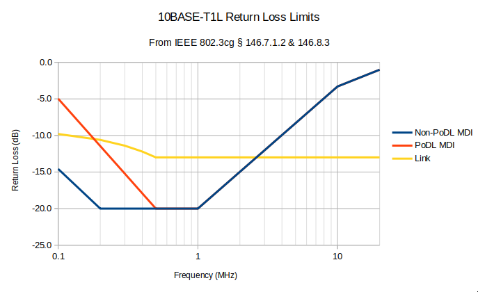
Return Loss Limits in IEEE 802.3cg
Note that there are two definitions of MDI return loss: One for a PoDL (Power over Data Line) enabled device and one for devices without PoDL support. The original 802.3cg-2019 specification only listed the non-PoDL limit which requires rather large power coupling parts (either discrete or coupled inductors). Return loss at the MDI depends on the reflection coefficient of the MDI in a 100 Ω system:
\[RL = 20log_{10}\left(\left|\frac{Z_L-Z_0}{Z_L+Z_0}\right|\right) = 20log_{10}\left(\left|\frac{Z_L-100}{Z_L+100}\right|\right) \text{ (dB)} \tag{7}\]So to achieve a return loss of -14.6 dB, the load impedance must be between 68.6 and 145.8 Ω. Since the PoDL coupling network will be in parallel, you can calculate the minimum impedance of the PoDL network by using the parallel impedance equation:
\[Z_L \ge 68.6 = \frac{Z_L*Z_{PoDL}}{Z_L*Z_{PoDL}} \rightarrow Z_{PoDL} \ge 218.5 Ω \tag{8}\]Assuming that two non-coupled inductor are used for PoDL, each must be greater than half of the calculated \(Z_{PoDL}\) value since they are effectively in series across the pair with their center point being a virtual AC ground. To achieve a return loss of 14.6dB at 100 kHz, the inductors must be greater than 174uH:
\[|Z_L|\ge 109.25 Ω=2πfL=2π100000L \rightarrow L \ge 174 µH\]PoDL class 15 supports up to 1.58 A; inductors that can handle 1.58 A without saturating take up a lot of space, and with there being no real signal integrity reason for keeping such a low return loss requirement at the MDI, people complained to IEEE. In 2022, IEEE task force involving Analog Devices responded to industry comments about the high cost of meeting this standard and proposed reducing the return loss requirement at 100kHz to 5 dB. This ended up being codified in IEEE 802.3dd-2022.
My circuit achieves about -8.5 dB return loss, but that is mostly due to my choice of an Ethernet transformer with magnetizing inductance of 200uH. I was disappointed that I had designed a non-compliant circuit initially (when I was only looking at a 2019 copy of the standard), but then I came across the 2022 changes and was relieved that my circuit was, in fact, compliant as an MDI that incorporates PoDL. Its a bit silly that the non-PoDL requirements are as high as they are — violating them but staying inside the PoDL return loss limits shouldn't cause any issues.
Design
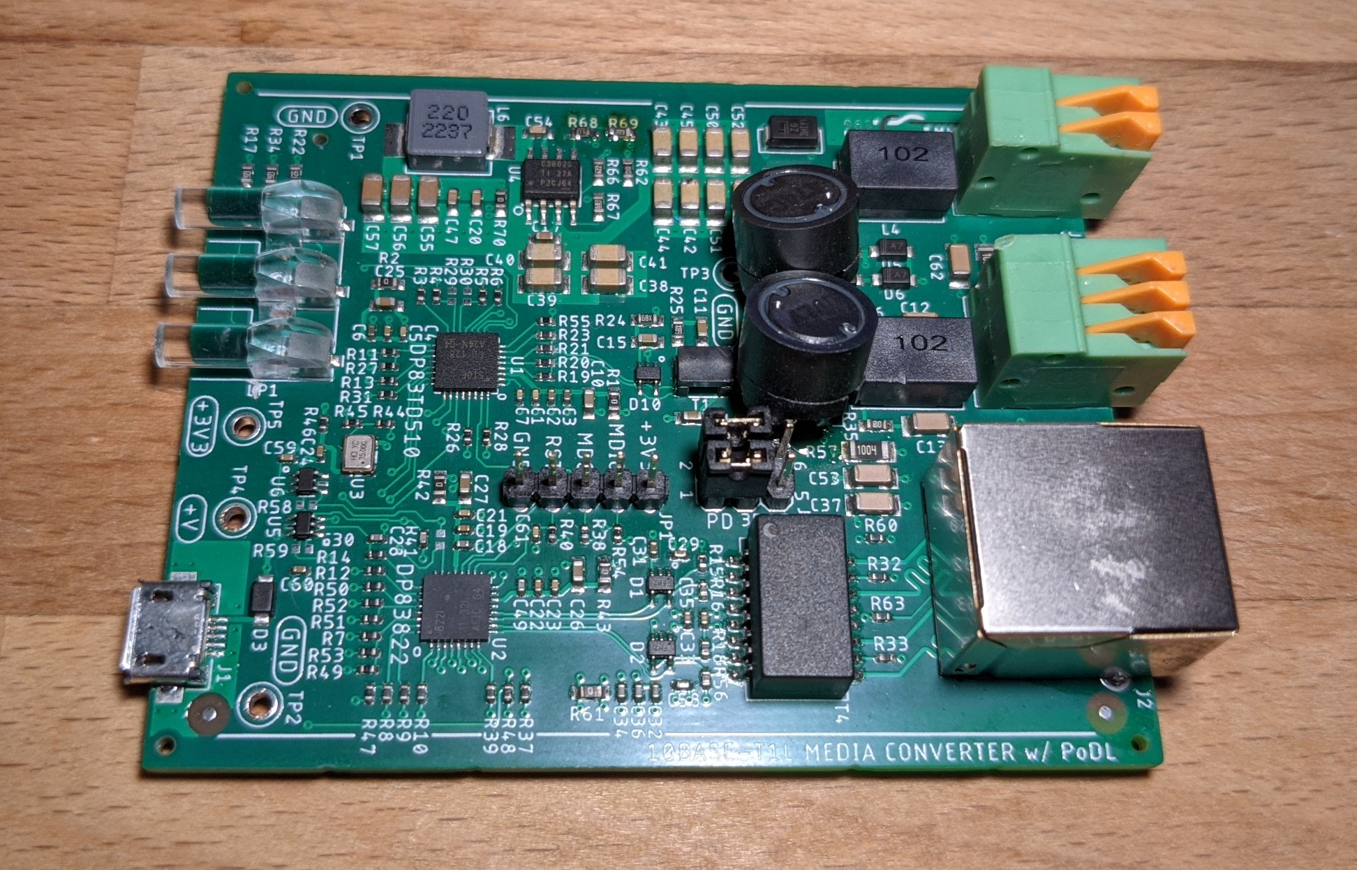
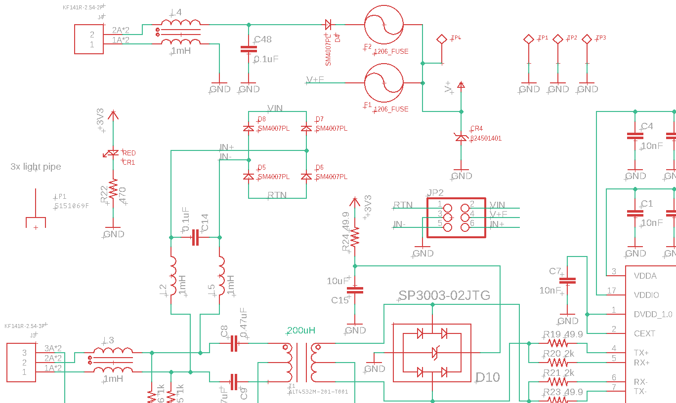
Project GitHub RepositoryThe heart of this project is a lightly modified reference design from Texas Instruments. The modifications include: PoDl sink and source support, a 5-60V buck converter, RGMII rather than RMII for PHY to PHY communication, and mechanical changes for a nice finished product. I ended up making three revisions of this project, so I will focus on the design of the final version and touch on the deltas between versions and the bringup process at the end.
Block Diagram
Media Converter
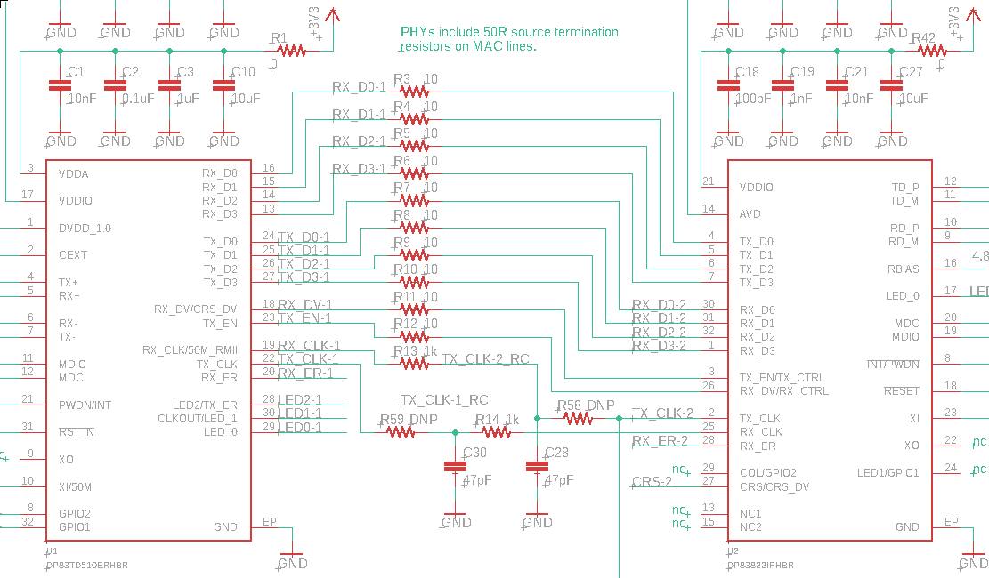
The actual media conversion in this adapter is performed by two TI Ethernet PHYs connected back to back with RGMII (Reduced gigabit media-independent interface). While it has 'gigabit' in the name, it can run at 10, 100 or 1000 Mbps. When operated at 10 Mbps, the data clock is 2.5 MHz which reduces power consumption compared to the other option supported by the DP83TD510 PHY for back-to-back operation, RMII, which uses a 50 MHz clock. The evaluation board for this phy, DP83TD510E-EVM, uses RMII, so this was a deviation from the reference design and a source of several days of pain during bring-up. Unlike most digital interfaces, the data clock for RGMII by default must be externally delayed to properly synchronize it with the transmitted data. Why is that the standard? I really don't know. It is possible to enable and internal delay (RMII-ID) to correct this, but with DP83TD510 the only way to enable the internal delay is over MDIO — it is not pin strappable. Instead of adding a microcontroller just to set this one register, I added an RC delays with Schmitt Trigger buffers to correct the clock skew in the second revision.
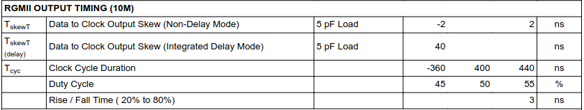
Data and Clock Transition Simultaneously by Default 🤦♂️
The two PHYs I selected were DP83TD510ERHBR (TI's only 10BASE-T1L PHY) and DP83822IRHBR (one of TI's many reasonably priced 10/100BASE-T PHYs). I included a transformer on the 10BASE-T1L side even though I could get away with AC coupling capacitors because for additional protection against line surges. Transformers inherently provide protection against common mode transients (they only let common mode due to parasitic capacitance between the windings) and protection against differential mode transients due to transformer saturation. You can only couple so much differential energy through before the transformer core saturates which limits the amount of power that has to be dissipated by protection diodes. 10BASE-T1L is designed for long cable runs where transient currents due to indirect lightning strikes are more likely to be seen, so I protected the inputs as well as I could short of adding gas discharge tubes (not enough room on the PCB). The 10/100BASE-T PHY implementation is pretty standard, but this PHY makes the interesting claim that it supports error free transmission of 100BASE-TX with 150m cable spans of CAT-5e. IJust as it is possible to design a PHY that exceedes the requirments of the spec for 10BASE-T1L, it is possible to dot he same for normal fast Ethernet.
Back-to-Back Ethernet PHYs
The two PHYs share a 25 MHz oscillator and are connected together with a bunch of 10 Ω resistors. I included these initially so that I has flexibility to bodge in a wire if I messed something up and as a handwavey EMI mitigation measure. The PHYs have 50 Ω source termination built in, so these resistors at the output of the drivers are unnecessary. Also not that the RX and TX terminology is backwards compared to what you might expect. The MII RX pins are outputs and the TX pins are inputs which ia why in the layout these resistors are located at the PHY RX pins.
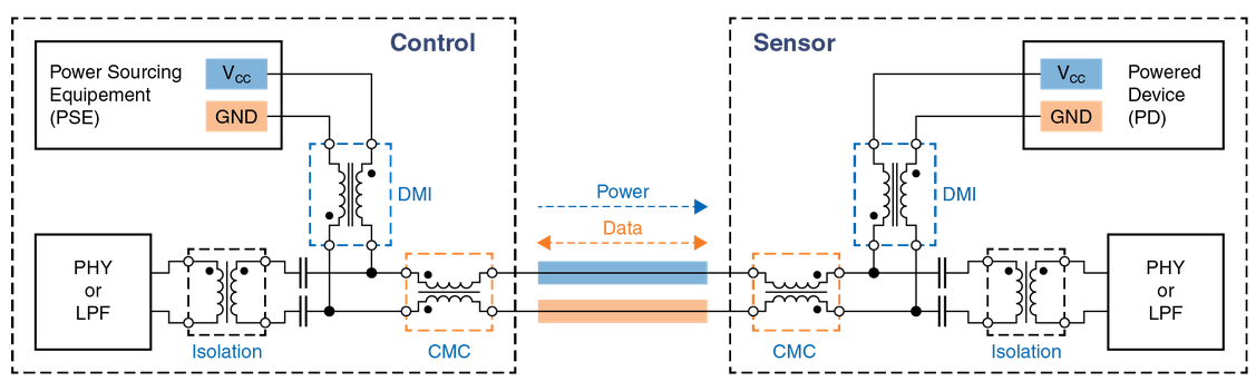
Power overt Data Line (PoDL)
Unlike normal Ethernet where you can use the center tap of the transformer to superimpose common mode DC power onto your data lines, with single pair Ethernet you must put differential mode power on a single differential data line. A transformer by itself would present a DC short, so you must add series DC blocking capacitors before the transformer. To tap power from the line, you need to either use two coupled inductors configured to block differential mode AC signal or you need to use two discrete inductors set up as bias-Ts. Using a differential mode inductor is more space efficient and lower loss, but you need to pick an appropriate part. TDK has some excellent options, but these were not stocked by JLCPCB, so I tried to be clever and use a common mode choke as a differential mode inductor. This can work (and I have done it on other products in the past), but it didn't work here (on rev2) for reasons I don`t quite understand. I haven't made a test coupon to measure insertion loss across frequency, but my best guess is that the common mode choke I selected (a Chinese part with a terse datasheet) has a rather lossy core and/or poor coupling between the inductors.
Nice TDK PoDL Parts that I Did Not Use
Since the power requirements of this board are super low (it is only powering itself), I could easily get away with using high-value discrete inductors for PoDL instead. I prototyped through hole 1mH inductors on the rev2 board and then designed surface mount 1mH inductors into the final board. At 5V, this board draws about 100mA, so I selected inductors with a saturation current 2x that. The actual footprint was still about the same as the common mode choke I tried to abuse into a differential mode inductor.
Rev2 Board with 1mH Inductors Bodged On
The impact of 1mH inductors on the AC performance of the circuit is negligible. I did not initially realize that you get a 2x win on inductance due to the fact that these inductors are effectively in series with each other across the differential pair, so that was a nice surprise when I went to calculate the actual return loss of my PoDL circuit including the transformer. I went with 1mH here instead of a smaller value because of the low magnetizing inductance of the Ethernet transformer that I chose. I realized only recently that you can have JLCPCB procure parts listed as out of stock — I had previously constrained myself to parts that they already had in stock which is why I selected the non-ideal transformer.
Rev3 PoDL Input Circuit
There are standards for negotiating device power class for 10BASE-T1L PoDL, but there aren't any ICs that take care of this power negotiation for you, so you have to implement it yourself using analog circuits and a microcontroller. TI has a detailed Application Note on this topic, but I decided to just implement passive PoDL: If you enable power from the PSE, there will be power on the line unless something shorts it out. To protect against that case, there is a series polyfuse. For low power devices like this, I think that is entirely adequate. Take a look at the TI App note if you're interested in implementing PoDL the standards compliant way.
Jumpers on header JP2 define whether a unit is the PSE (power sourcing equipment), the PD (powered device), or if PoDL is disabled. The PSE supplies power to the single pair line and the PD draws power from the single pair line. When the jumpers are in PD mode (pins 5 and 3 shorted & pins 6 and 4 shorted), the board's power and ground rail are powered through a bridge rectifier that makes the connection of the single pair cable polarity insensitive. When the jumpers are in PSE mode (pins 1 and 3 shorted & pins 2 and 4 shorted), the bridge rectifier is bypassed and power is directly applied to the inductors. In both cases the line connects to the power rail on the board through a polyfuse.
Diode D4 protects against reverse polarity on the input power connector and diode CR4 protects against overvoltage transients. The polyfulse will limit current during sustained reverse power connection. If diode D4 were removed and shorted, it would be possible to power remote equipment through the input power connector.
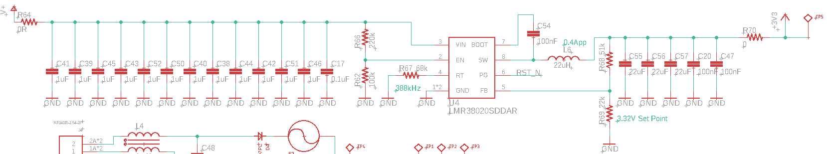
Power Supply
Impressive progress has been made in recent years with integrating and miniaturizing high voltage rated buck converters. Ten years ago, I designed a board with a LM5008 buck converter. This is a 95V rated 0.35A capable integrated switcher. It has a quirk, though: it requires high output ripple to stabilize its control loop, so you need to put a resistor in series with your bulk output capacitor. At 48Vin and 10Vout, it claims to be 87% efficient with a 0.3A load. Due to the required series resistance, the output voltage is load dependent to the tune of 1% per 0.1A.
3.3V Power Supply
I was generally dissatisfied with high voltage integrated bucks that I had used in the past, such as LM5008, so I looked for a new one for the project. I was pleased to find a brand new part from TI that I had not run into before: LMR38020. This is an 80V rated 2A capable integrated switcher with a claimed efficiency of 91% at 2A out. This part also employs pulse frequency modulation to achieve high efficiency at low load, and it doesn't have any strange requirements like having a high output ripple. With this part, I was able to design a 3.3V regulator that was happy to get anything between 5V and 75Vin which allowed me to power this board off of USB, off of an auxiliary input, or over PoDL.
There weren't any recommended values for a 48V to 3.3V implementation, so I iterated a bit from the 5V recommended values and picked passives that matched basic parts on JLCPCB. JLCPCB has a pretty slick operation for PCB assembly. They have designated some of the most commonly used parts as 'basic' parts and seemingly leave them loaded in their pick and place machines at all times. You art not charged a setup fee for using basic parts, but if you use an `extended' part (most everything else they have in stock), you are charged a $3 setup fee per part. This provides a strong incentive to use basic parts where possible which is why I used a dozen 1uF 1206 50V X7R capacitors for bulk input capacitance rather than using, say, three 4.7uF 1206 capacitors: The 1uF parts are 'basic' parts. If you're ordering five boards:
- 12x 1uF 1206 Capacitor
- Setup Fee: $0
- Extended price: 5x12x0.0158 = $0.95
- Assembly Fee: 5x12x2x0.0017 = $0.20
- Total: $1.15 = $0.23 / board
- 3x 4.7uF 1206 Capacitor
- Setup Fee: $3
- Extended price: 5x3x0.0425 = $0.64
- Assembly Fee: 5x3x2x0.0017 = $0.05
- Total: $3.69 = $0.74 / board
Once you're building more than prototype quantities of boards, the benefit of optimizing for basic parts disappears, but I never build that many boards for personal projects, so I use them where I can such as in the feedback divider for this power supply.
I went with a slightly larger inductor value than recommended to improve efficiency (less current ripple = less core loss) since my load is pretty light, and I used a bit more input and output cap than in the recommended implementation in the datasheet. Since a power supply at the end of a few thousand feet of 24 AWG wire will see significant input voltage droop under load, extra input cap can help protect against instability. Imagine that you have a power supply with no input cap, significant output cap, a current limit of 2A, a fast control loop, and no soft start functionality. When you first turn this part on, it will immediately draw up to the 2A current limit as it tries to charge the output cap. If there is 100 Ω of series resistance between the input on this supply and whatever is powering it, the input voltage will quickly collapse to 0V became you can't draw 2A through 100 Ω if the source voltage is only 48V. What you've made is an oscillator, not a 3.3V regulator. Input capacitance (as well as soft-start and having only small load transients) prevents this oscillation.
Described more technically, buck converters have negative input impedance at low frequencies. If the impedance of the input filter (or long cable in this case) exceeds the absolute value of the converter's input impedance at any frequency (both are frequency dependent), your system will oscillate. This is known as the "Middlebrook Criteria," and it is described in detail in R. D. Middlebrook's 1976 paper.
Layout
I designed this on a four layer board from the start. You have to swizzle the connections between the two PHYs, so there is a lot of having to cross over other traces which is best to do with a four layer board. I preferentially tried to route horizontal traces on layer 4 and vertical traces on layer 1. There are many exceptions to these rules, of course, but if you start doing vertical routing on the horizontal routing layer you will quickly find yourself blocked. The PHY-side Ethernet pairs are tightly coupled differential microstrip traces while the connector side Ethernet pairs are loosely coupled. A Loosely coupled differential pair is one where the single ended impedance of each trace predominantly defines the differential impedance and there is relatively little trace to trace coupling. Tight coupling gives you better common mode interference rejection and uses smaller traces, but if the two traces stop being tightly coupled (such as when you have to break out of a BGA or when you tune one side of the pair) you will get an impedance discontinuity. With a loosely coupled pair, you are free to change the distance between the traces without creating a large discontinuity. On this design, the PoDL circuity and length matching for the RJ45 connector warranted the use of loosely coupled traces on the connector side of the transformers.
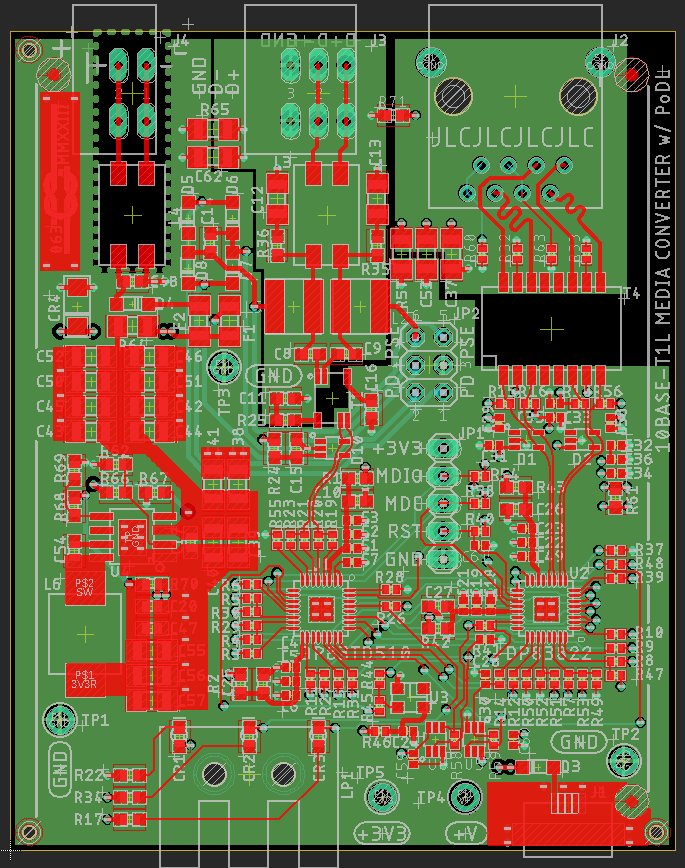
Rev3 Layout
I used three different ground planes in this design since I have isolation transformers for both Ethernet interfaces. I was careful to not route anything but power across the gaps in these planes and voided all layers under the transformers to reduce parasitic capacitive coupling to the windings. The power supply was laid out roughly following the recommendations of the datasheet. With buck converters you want to try and keep the loop area between the input capacitor and the power and ground pins of the switcher as small as possible since this is where you will dee the highest di/dt. The output loop is less critical, but it doesn't hurt to minimize it as well where you can.
The ground and power test points scattered around the board are not populated by default, but the ground test points can be quickly soldered in if you need to probe around with an oscilloscope. I recommend including ground test points like this on all designs — you may end up using them to pass a bodge wire from one side of the board to the other.
Mechanical Design
Finding good enclosures is hard. I wanted a small aluminum enclosure with card guides, so I went with the same one as I used for my USBC Charger which is $9 on Amazon. The main PCB slides into the card guides, and then PCB end places are screwed onto the ends of the box to complete the enclosure.
Two Rev2 boards in an Enclosure with One Powering the Other
I included three status LEDs: One red power LED, a 10BASE-T1L activity light and a 10BASE-T activity light. These LEDs interface with the front panel PCB plates through plastic light pipes — in the final revision of this board, the board comes fully assembled except fot the plastic light pipes.
Rev1 Board
I went through two options of wire to board connectors. I started with a screwless terminal block from CUI, but JLCPCB didn't have that part in stock and I didn't really like the look of it. On rev2 and rev3, I used a spring clamp part from a Chinese manufacturer which meant that the boards could now be 100% assembled by JLCPCB.
Design Progression
One of the main reasons that I do personal projects like this is to learn about things I haven't run into yet with my day job. Making a design mistake here (aside from teh careless errors of which there are plenty because I don't take much time to review my personal projects) means that I am going to learn something. Here's the summary of what changed across the three revisions of this design:
- Rev1 Issues:
- No RMII clock skew insertion.
- Wrong 3.3V buck voltage divider.
- Oversized 3.3V buck inductor.
- Swapped RX pair polarity on 10BASE-T PHY.
- Missing strapping resistors.
- Inappropriately small series common mode choke.
- Totally wrong PoDL inductor configuration
- Rev2 Changes and issues:
- Added clock delay circuit.
- Forgot to fix the 3.3V buck voltage divider.
- Reduced 3.3V buck inductor size.
- Fixed RX pair polarity on 10BASE-T PHY.
- Changed RJ45 pinout to MD-X
- Fixed strapping resistors.
- Increased series common mode choke size for both data lines and input power lines.
- Implemented differential mode inductor for PoDL (this was ineffective).
- Changed to 0402 passives where possible.
- Changed wire to board connectors to a cheaper more ergonomic option.
- Modified assembly to be 100% by JLCPCB.
- Added clock strapping option to support RMII (untested)
- Rev3 Changes:
- Fixed 3.3V buck voltage divider.
- Changed to a discrete inductor PoDL implementation.
- The boards were fully functional out of the box!
The most annoying issue I encountered was the requirement that an external clock skew be applied with RGMII. It took several evenings of tinkering across a couple weeks for me to sort this out. I was able to get the 10BASE-T PHY to show a valid connection, but I could never get a packet through end to end. Both of teh PHYs on the board have a variety of loopback test modes to help with debugging and I had had the foresight to break out the MDIO control interfaces of the PHYs to headers, so I was able to use an ESP32 and some crappy Arduino code to command the 10BASE-T1L into a loopback mode. I started with MII (Media Independent Interface) loopback since it is the first stage in the part and was happy to see data coming out of the RX RGMII data pins.
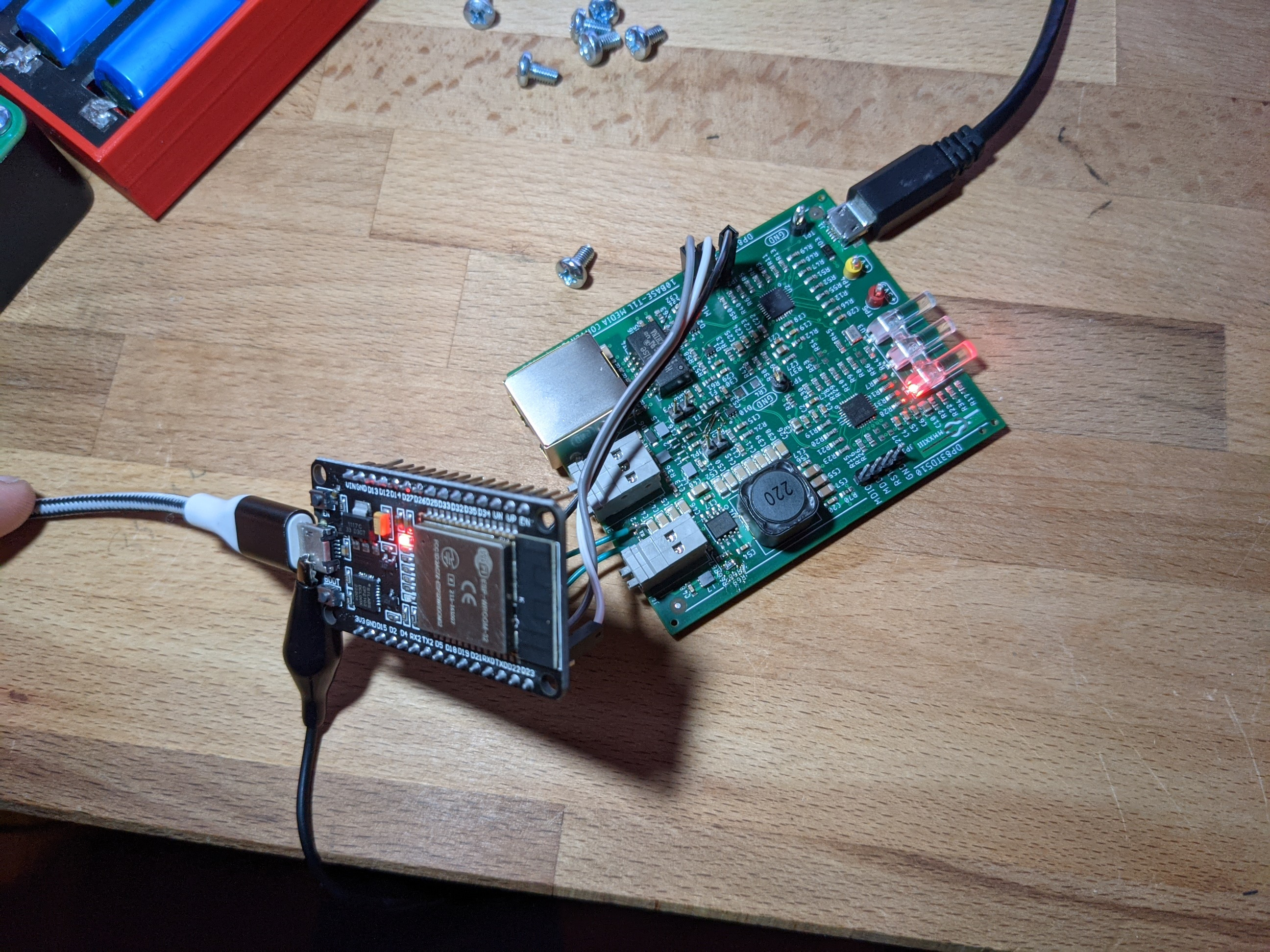
ESP32 as an MDIO Debugger
At first it just looked like a time delay was being added (as one would expect), but then I decoded the data by hand and compared it to the TX data. I found that the PHY was changing the data deterministically: It changed the first one in a sequence of ones into a zero! So if you sent 0111 0111 0111 0000, you would receive 0011 0011 0011 0000. After sleeping on that finding, I realized that there may be an issue with the clock. What I had assumed was a falling edge synchronized clock was actually a rising edge synchronized clock that rose at the same time as the data. I then found the line in the datasheet about internal and external delay mode and used teh ESP32 dongle to enable internal delay mode on the 10BASE-T1L PHY on both boards and for the first time had data running through the media converters.
Finally Passing Data Between Two Thinkpads
These parts have no internal memory, so it is necessary to program them every time you power them on if you have to change a register that isn't set through a pin strapped register. Annoyingly, you can't use pin strapping to set the internal delay register, so I had to add my own external delay. I thought about implementing it with a long wire, but with a 25MHz clock, that would be a pretty long wire. Since this clock isn't particularly phase noise sensitive, I instead added an RC delay to slow down its edge a bit. This worked fine, but I didn't like having to rely on the internal input high threshold of the PHYs to define the amount of skew, so I added a buffer circuit to rev2 to provide a nice square delayed clock signals between the two PHYs.
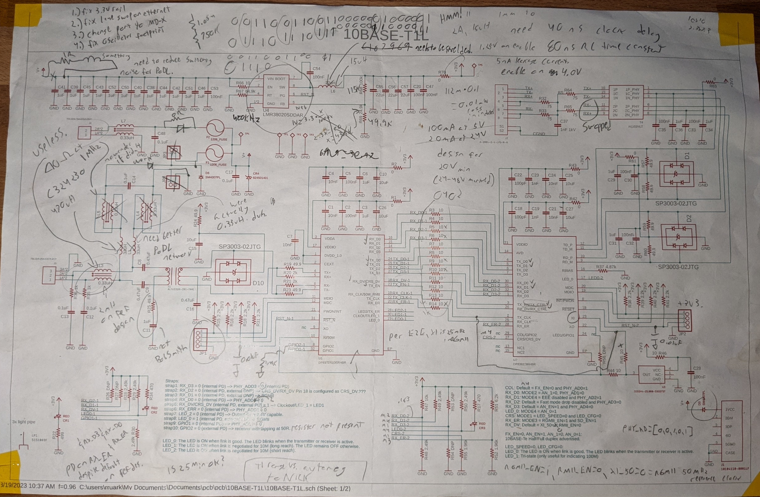
Notes on the Rev1 Schematic
I design all of my schematics for 11x17" paper and make a point of actually printing them out when I bring up a new design. I find that it is a lot easy to document everything that you want to change and to keep track of what you've double checked if you can physically mark it on paper. Its worth a quick trip to the FedeX store to get your schematic printed full size.
The first two PoDl networks were ineffective, but I think I've covered this enough already in the rest of the writeup. Advice: simulate your return loss and build test coupons to measure return loss if you're going to get clever with coupling networks. The other power and strapping mistakes easy to quickly identify and correct.
Rev3 Boards as They Arrive from JLCPCB and Added Light Pipe
In order to enable PoDL on the final boards and define them as PSE (power sourcing equipment) or PD (powered device), you have to install a 2x3 header and add appropriate jumpers. The boards otherwise arrive fully functional from JLCPCB.
Conclusion
I started this project partly because there doesn't exist a reasonably priced 10BASE-T1L media converter on the market. The parts are not terribly expensive it just seems that this is a niche product. The all-in cost of a run of five of my boards from JLCPCB was $185 (inclusive of tax and shipping). Adding in the $1.20 light pipe (highway robbery for a piece of clear plastic), $0.50 for end places, $0.10 for screws and $9 for the case, that is $48 each which is not bad at all for such a limited run. I imagine that cost would drop to ~$30 for a run of 100 especially if a more direct source of enclosures could be found.
Completed 10BASE-T1L Adapters
I'm not selling these, but the design is open source meaning that anyone can take the files off of Github and build some of their own.
'Competitor' Products
- $250: Honeywell 10BASE-T1L-ADAPT
- $224: SPEBlox-Long
- $178: TI DP83TD510E-EVM Evaluation Board
- $160: Altronix PACE1KL
- $86: Analog Devices 10BASE-T1L-MC Reference Design
- $?: Datamate DM7980
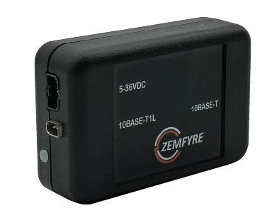
- $?: ZEMFYRE ZM101LP
The Altronics box is the minimum viable adapter on the market that isn't a bare PCB. The Datamate and Zemfyre options look nice, but you can't pull out your credit card and buy them today.
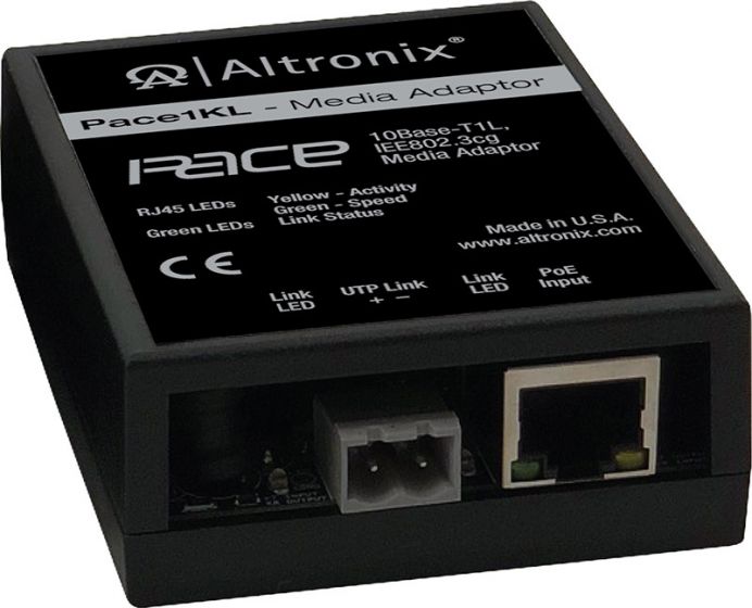
Altronix PACE1KL
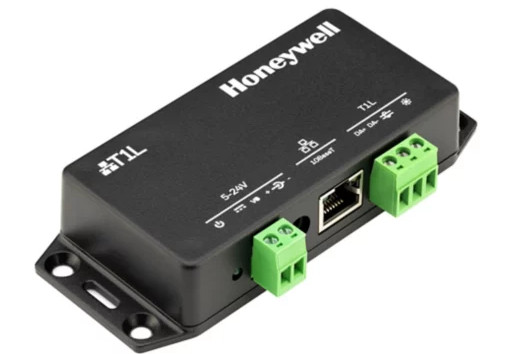
Honeywell 10BASE-T1L-ADAPT
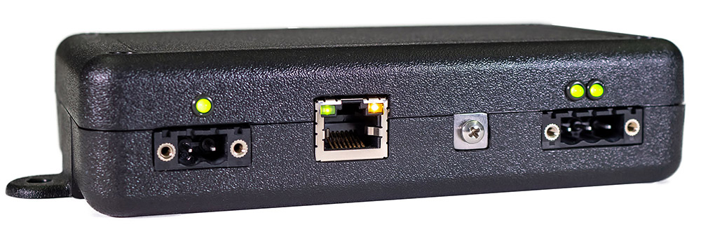
Datamate DM7980
ZEMFYRE ZM101LP