Decent SMA Transitions
2023
PCB to coax RF transitions are tricky. Many edge-launch SMA connector datasheets do not include recommended footprints, and those that do are often designed for two layer boards. If you take a footptint designed for a two layer board and put it on a four layer board, you will have terrible performance due to the added capacitance of the pad to the inner layer ground plane. After coming up empty handed for years when searching for practical — measured — transitions for use with the most common stackups that electronics hobbyists are likely to use, I decided to design one myself through trial and error. Typically the first step in designing such a transition would be simulation, but the price of EM simulation software puts it out of reach to hobbyists that don't have access to it through work or school. I instead made some back of the envelope calculations based on treating the signal pad of an SMA transition as a grounded coplanar microstrip line and iterated from there.
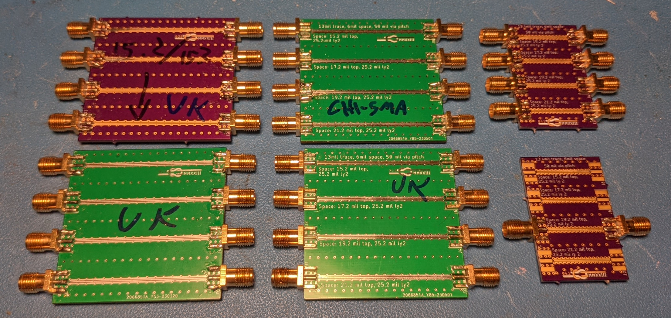
Two Iterations of JLC PCB and OSHPARK SMA Transition Test Boards
The four layer FR408HR stackup from OSHPark hasn't changed in years, but yet I can't find a single practical implementation of a edge launch SMA transition for this stackup. There are some papers on simulations of transitions, but nothing with good real-world results. This project seems to have been abandoned with the a picture in the gallery showing poor performance (10dB return loss at 3 GHz). There is a nice project that determined an effective 50 Ohm grounded coplanar waveguide design, so I used that for the line between the SMA connectors. This FMCW (Frequency-Modulated Continuous-Wave) radar project includes simulations of an SMA transition, but no measured performance.
YARD Stick One SMA Transition (No Inner Layer Voiding)
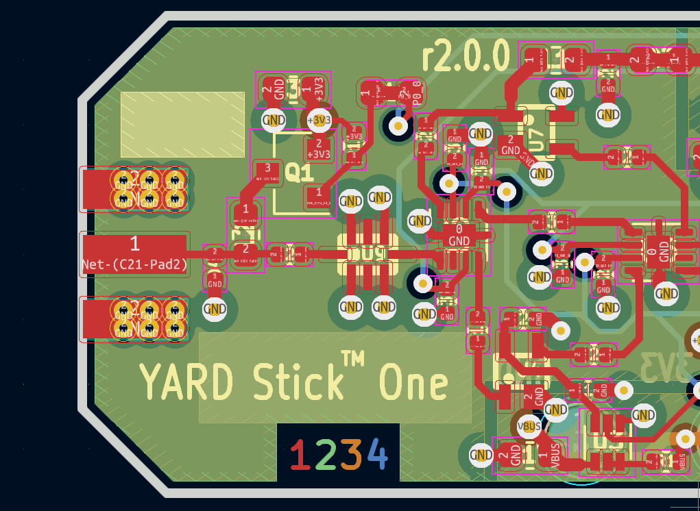
Open source RF projects like HackRF One and YARD Stick One appear to have pretty non-ideal SMA transitions. HackRF One voids all layers under the SMA RF pad which likely presents an inductive discontinuity while YARD Stick One voids no layers which certainly presents a capacitive discontinuity. My goal with this project was to produce a tested 'recipe' for an SMA connector that can be copied by anyone designing a simple RF board using OSHPARK or JLC PCB.
Design
I decided to come up with transitions for two popular PCB suppliers: OSHPark and JLCPCB. OSH park has a single standard 4-layer stackup while JLCPCB offers a number of options. I selected the JLCPCB stackup most similar to the OSHPark stackup: JLC04161H-7628. This stackup also seems to be the default stackup when impedance control is not selected (the stackup preview shows the same dimensions), and I did not select impedance control on my first order and the performance matched.
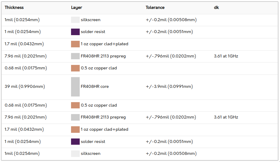
OSHPark 4- Layer Stackup
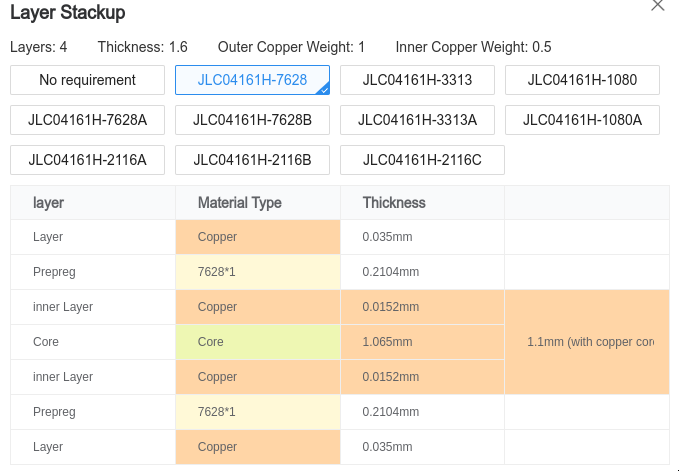
JLC04161H-7628 4- Layer Stackup
I used a 13.4 mil wide trace with 6 mil spacing to the ground plane and 12 mil vias spaced every 100 mil for the grounded coplanar waveguide trace between the two SMA connectors following the results of this project. The linked project used 50 mil via spacing with 13.77 mil vias but I changed it to 12 mil vias with 100 mil spacing because this paper suggests that tighter via pitch won't really improve performance (aside from crosstalk) below 20 GHz and because I almost exclusively use 12 mil vias in my projects. The main reason to remove soldermask from the trace is that the thickness of soldermask is not well controlled between batches, so even if you find the ideal trace geometry on a single board, performance is liable to degrade if the same design is manufactured a second time due. For the JLC board, I scaled the trace down to 13 mil in alignment with the higher dielectric constant and lower thickness of the JLCPCB stackup.
I chose CON-SMA-EDGE-S from RF solutions as the edge launch SMA connector because it is the cheapest available on Digikey ($1.69) and because its dimensions are quite close to DL-SMA-K513-08K from DEALON which is a cheap ($0.21) equivalent from LCSC. There are no recommended footprints for CON-SMA-EDGE-S and DL-SMA-K513-08K, so I made one up:
Common CON-SMA-EDGE-S and DL-SMA-K513-08K SMA Connector Footprint
I sized the center RF pad the same size as the width of the signal pin on DL-SMA-K513-08K (1mm). CON-SMA-EDGE-S has a thinner pin (0.76mm). You could made the pad proportionally smaller, but you may run into issues with variability in performance when the connector is slightly offset on the bad. You also typically want pads to be larger than pins so that there is room for the solder to fillet between the pin and pad. Solder fillets make for stronger and more reliable joints and they also make it easy to inspect the joints.
While using a 1mm pad for both connectors means that DL-SMA-K513-08K won't have much of a solder fillet (and I did have to be more careful soldering them), the Keeping the pads the same also allows for the same transition design to be used for both connectors without giving up much performance.
Grounded Coplanar Waveguide Starting Estimate for Transition
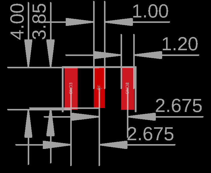
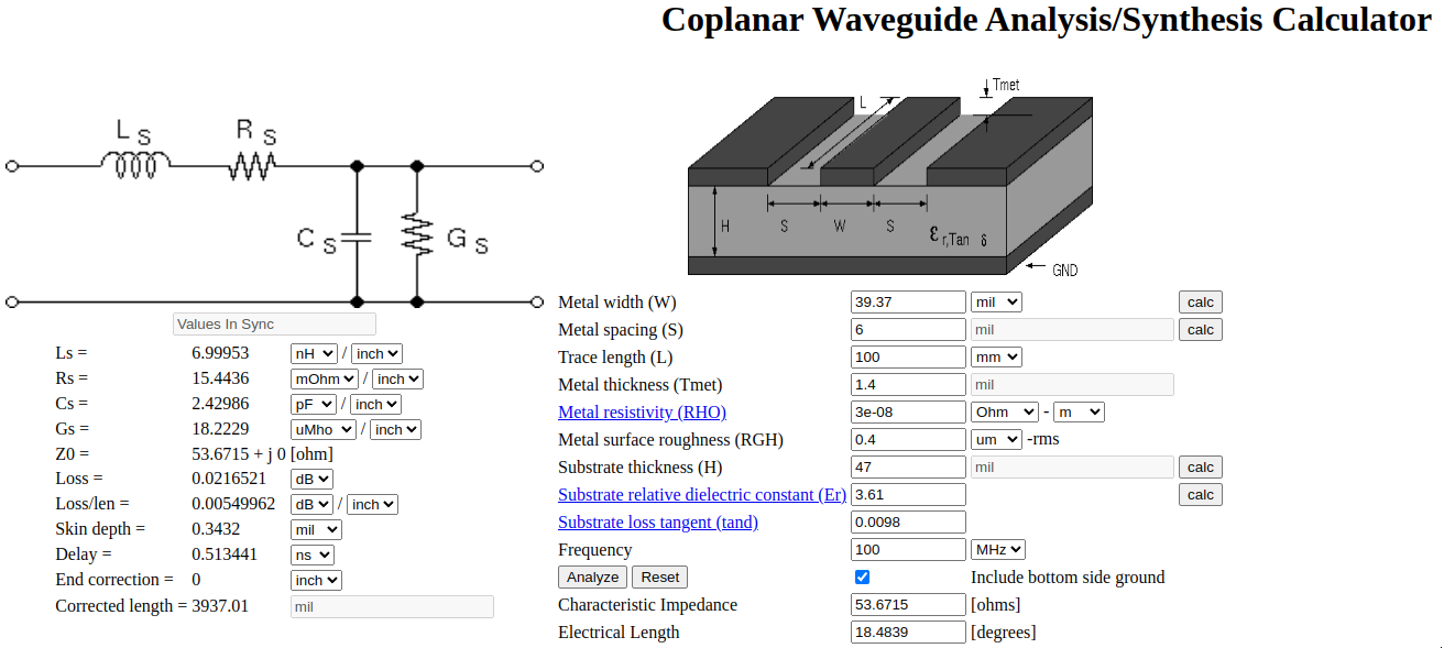
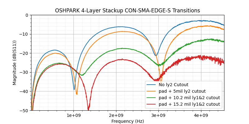
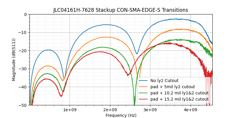
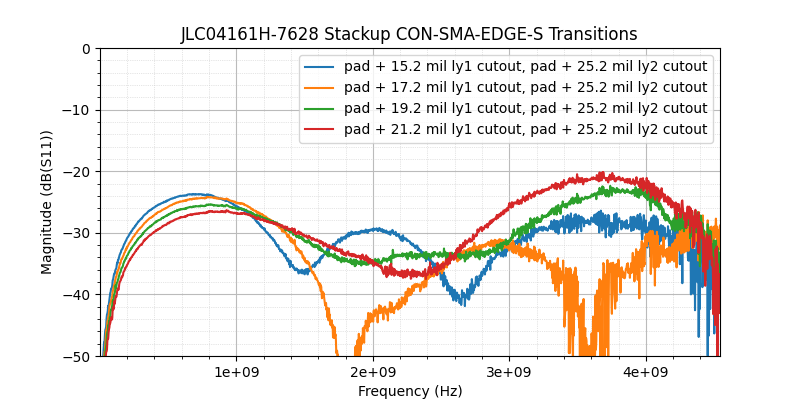
For the SMA transitions, I started with a guess based on a grounded coplanar waveguide calculator with the width of the SMA pad entered as the width of the trace. This calculator suggested that only an inner layer cutout and no additional pullback (just the default 6 mil clearance) on the top layer would bet me pretty close (54 Ohm), but I figured the height of the pin above the PCB would add additional capacitance, so I built a board with two additional pullback options: 10.2 mil and 15.2 mil. The 15.2 mil setback option ended up having the best performance, so I designed a new board with a pad + 25 mil cutout on layer 2 and with 6-21.2 mil pad to ground spacing on the top layer. I designed a total of six boards for this project: three OSHPARK boards and three JLCPCB boards. The third board from each also has a cutout on layer 3, but that ended up not showing any improvements over just having wider spacing on layer one with a layer two void, so I did not make any detailed measurements on those boards.
Here is the transition design that ultimately had the best performance. All dimensions are in mm. The signal pad is the same as shown in the footprint earlier. I designed the footprint in mm and the board in mils, but Eagle is weird about dimensioning (it doesn't snap to edges) so I just got it to the closest mil in the dimensioned drawings below.
SMA Connector Transition Design Top Layer
SMA Connector Transition Design Inner Layer Cutout
I left an 8 mil gap to the edge of the board to respect the trace routed to board edge requirement of JLC. You could push things closer and get marginally better performance (this gap in the ground plane adds a bit of inductance), but production fab houses often do not want copper touching the edge of the board because it can get messed up when the board is routed. The 10 mil gap at the pad to trace transition is arbitrary. You can taper the pad to trace simulation, but this starts getting into territory where you really need to be doing simulation since you are adding several more variables to optimize. Tapering is explored in this Altium Design Note, but the results actually show tapering degrading performance (probably because of the added capacitance in the tapered region). Their untapered result (simulated, not measured) is also worse than my measured result, so the design presented is definitely not optimized.
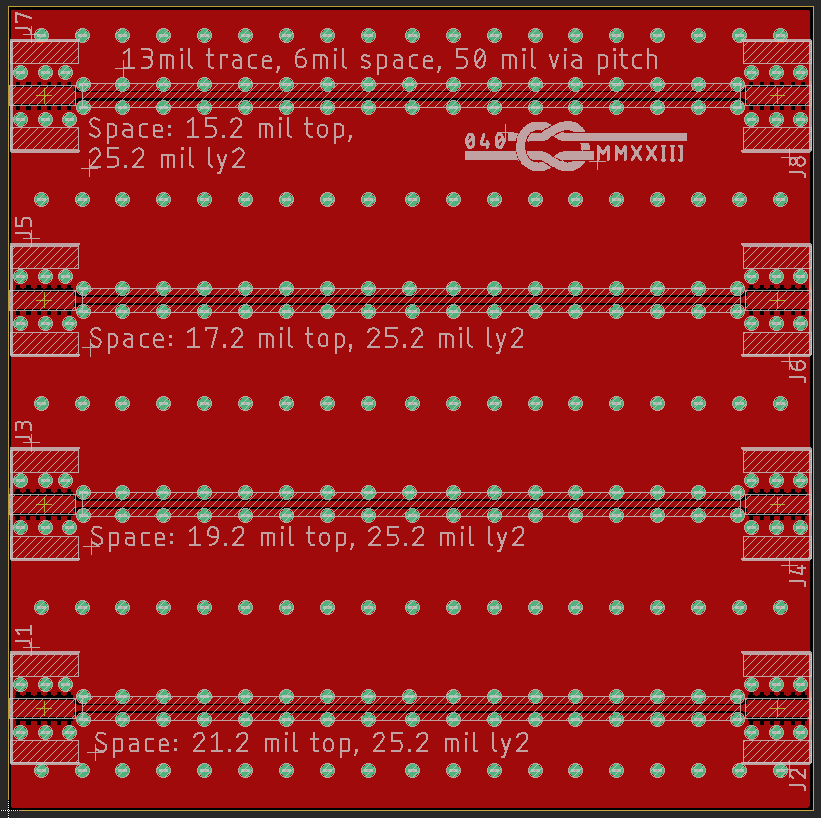
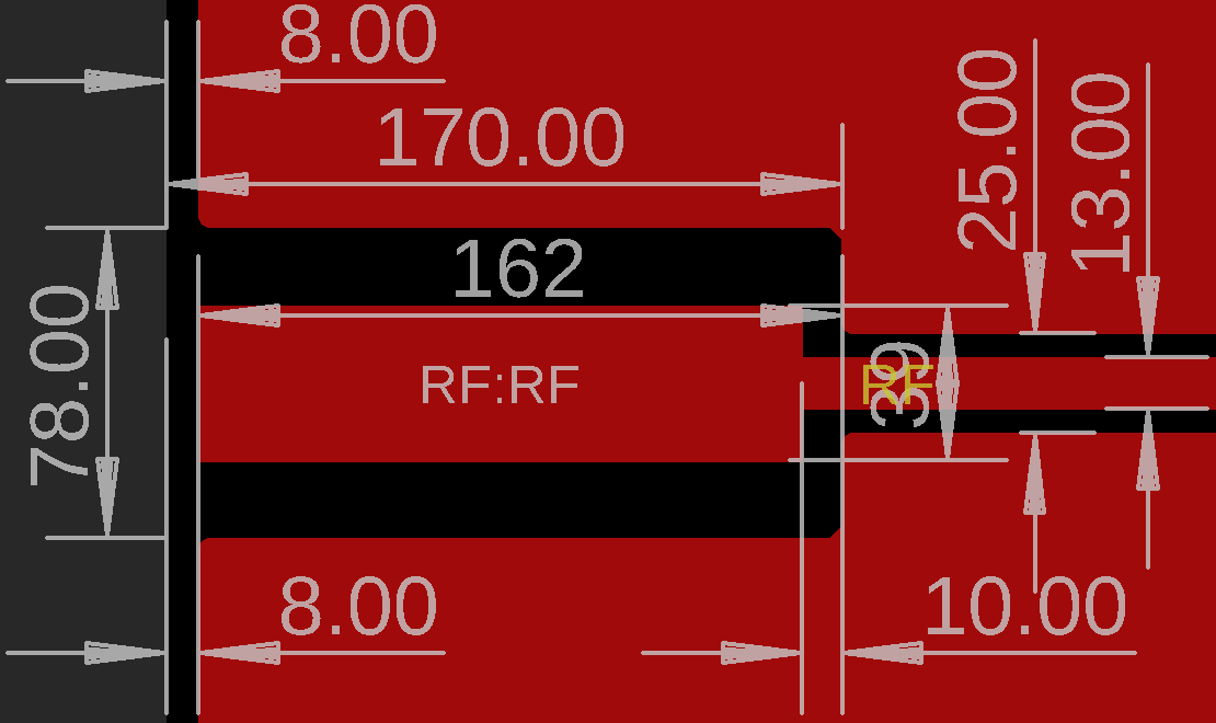
Second JLCPCB Test Board Layout
The Eagle schematic and PCB design files as well as the Gerber exports for the boards ordered from JLCPCB can be found here. Note that while the boards say the via pitch is 50 mil, it is in fact 100 mil.
Results
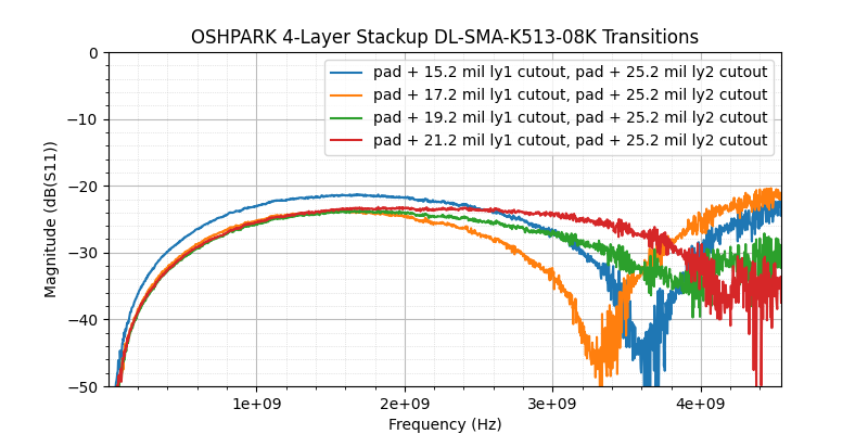
I achieved acceptable performance on the first iteration of the OSHPARK board (<-20dB S11 from DC to 4.5 GHz), but the JLC PCB board wasn't quite there (-16dB S11 at 3.4 GHz). I lucked out on the second round of boards: I found a single footprint that works acceptably for both CON-SMA-EDGE-S and DL-SMA-K513-08K on both OSHPARK and JLCPCB JLC04161H-7628 four layer stackups! Here's a comparison of the results of this footprint on the various boards compared to the original untuned footprint:
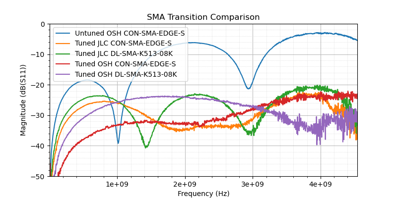
Comparison of SMA Transition Performance on Two Stackups with Two Connector Parts
Note that this is the composite return loss of the two connectors back to back. The actual return loss of a single transition into a matched circuit on a PCB will be ~6dB better than the worst case composite return loss plotted here. This means that all of the tuned transitions shown actually have a return loss of <-26dB from DC to 4.5 GHz which is a VSWR of <1.11 if you prefer that terminology.
I reduced the trace length on the second rev of the OSHPARK boards to save a couple dollars (board width reduced from 50mm to 27mm) which is why they show a flatter response. Since these are through board tests (the termination resistor is not on the board itself), you see the effect of reflections at both SMA transitions. At some frequencies, these interfere constructively (resulting in worse return loss) and at some frequencies these interfere destructively resulting in better return loss. Since the second rev of the OSHPARK boards has a shorter trace between the connectors, you don't see the first destructive interference until a bit less than twice the frequncy seen on the first rev of the baord.
The untuned footprint on the first rev of the boards can be roughly modeled as a simple 1pF shunt capacitive discontinuity:
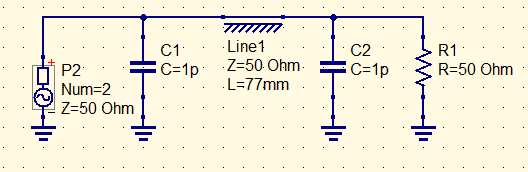
QUCS Schematic of 1pF Discontinuity
The boards have a physical distance between connectors of about 42mm between the two connector pads, but the simulation above shows 77mm. This is because the velocity factor (fraction of the speed of light signals propagate at) of a transmission line is a function of dielectric constant:
\[V_F=\frac{1}{\sqrt{ε_r}}\tag{1}\]In grounded coplanar waveguide, some of the electric fields are in the PCB dielectric and some fields are in free space above the trace fringing to the ground planes to either side of the trace. This means that the effective dielectric constant of the trace is lower than the dielectric constant of the PCB laminate. This calculator predicts an effective dielectric constant of 3.2 for the 13 mil trace on the JLCPCB boards. This means that a trace with 42mm electrical length will have a physical length of \(\sqrt{ε_r}\)*42=75mm which is pretty close to the 77mm required to match the simulation to real world results.
The first null of the return loss plot corresponds to the frequency where the transmission line between the two connectors is a bit less than a quarter wavelength. The second null corresponds to a bit less than 3/4 λ, and the third null is a bit less than 5/4 λ.
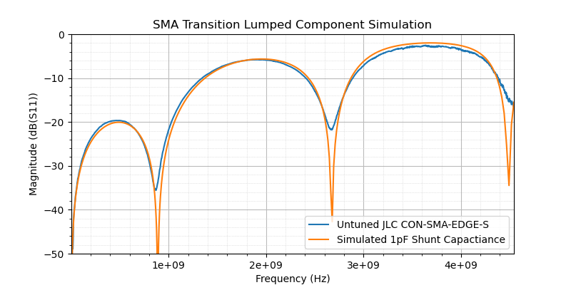
Untuned SMA Transition Compared to a 1pF Shunt Capacitive Discontinuity
This effect is best understood with a Smith Chart. Starting from the 50 Ω load, the capacitive discontinuity of the first SMA transition moves the impedance counter-clockwise along the line of constant conductance:
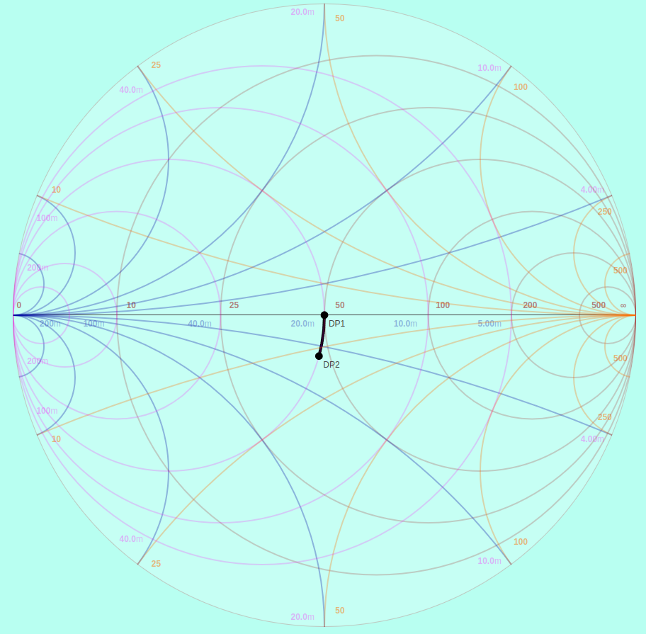
Effect of 1pF Shunt Capacitance at 850 MHz
This is a 50 Ω Smith chart, so lengths of 50 Ω transmission line from the load to the source (the VNA) rotate the impedance clockwise around the chart. A bit less than λ/4 of transmission line flips the sign of the imaginary part of input impedance and brings you back to the other side (inductive reactance) of the line of constant conductance:
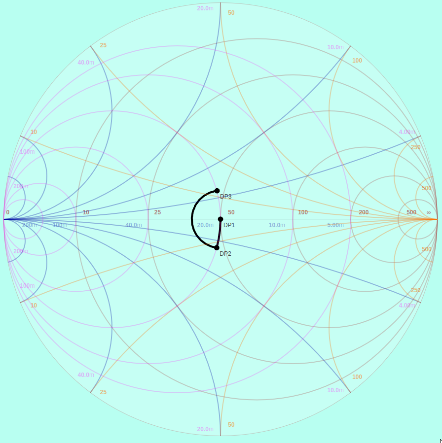
1pF Shunt Capacitance Transformed by Transmission line
The same capacitance then brings the input impedance back to the origin (50 Ω) following, again, the line of constant conductance:
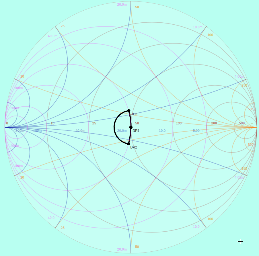
Two Capacitive Discontinuities Cancelled out by ~λ/4 Transmission Line
You see the next null around 3/4 λ because λ/2 brings you 360° around the chart and back to the inductive side of the circle of constant conductance. The impact of the capacitive discontinuity is greater at this frequency (about 2550 MHz for this board), but it cancels nonetheless:
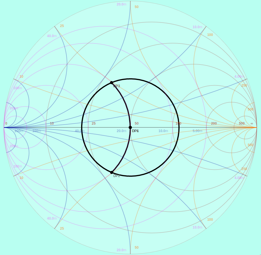
Two Capacitive Discontinuities Cancelled out by ~3/4λ Transmission Line
Worst case constructive interference is seen midway in between these nulls. A λ/2 transmission line brings you right back to where you started with the first discontinuity which makes the second discontinuity stack right on top of the first:
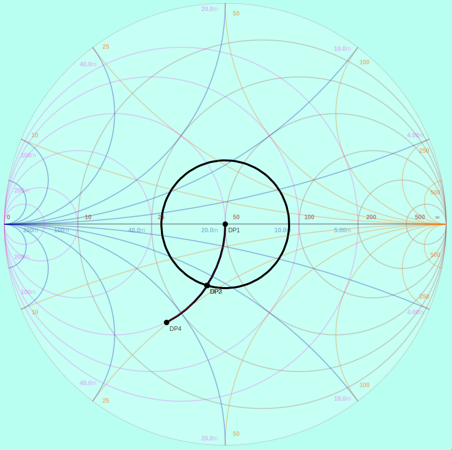
Additive Effect of Two Capacitive Discontinuities from a λ/2 Transmission Line
Microwaves101 has an excellent page describing this and other quarter wave transmission line effects.
Detailed Results
Measured S-Parameters for all of these plots can be found here. I plotted these in Python using matplotlib and scikit-rf. The python scripts that plotted these graphs can be found here.
Results of the Four Traces on the First OSHPARK Board
Results of the Four Traces on the First JLC PCB Board
Results of the Four Traces on the Second JLCPCB Board with CON-SMA-EDGE-S SMA Connectors
Results of the Four Traces on the Second OSHPARK Board with DL-SMA-K513-08K SMA Connectors
I didn't bother to populate CON-SMA-EDGE-S anywhere but the third option (19.2 mil top layer spacing) on the second OSHPARK board, so you can see its performance in the overall comparison.
Measurement Setup
All of these measurements were made with a NanoVNA V2 Plus using NanoVNA Saver running 15 sweeps with this configuration:
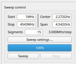
NanoVNA Saver Configuration
I calibrated the VNA to the end of the cable and connected the 50 Ω calibration reference to the output of the test coupon boards.
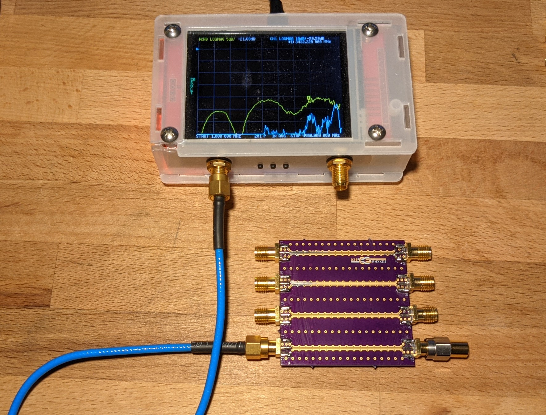
Test Setup
I could have terminated the trace on the board with an 0402 resistor, but then I could have potentially had an unknown discontinuity from the termination resistor. I decided instead to live with the known discontinuity of a second SMA connector. Now that I have a decent footprint, I will build some boards that terminate the trace in various shunt connected surface mount footprints to use as a test fixture to measure surface mount capacitors and inductors. You won't have much luck measuring an 0402 1pF capacitor with a bench LCR meter, but a VNA can measure such components quite accurately.