Solar Car Maximum Power Point Tracker
2015-2017
As a member of the Solar Car Team at Missouri S&T, I lead the project to design and build Maximum Power Point Trackers (MPPTs) to interface the car’s 36V solar panels to its 130V battery.
SchematicLayout
We had been using very high quality MPPTs , but the team was looking to move to a car design that would require more sub-arrays and thus more MPPTs. Any product targeted at a niche market that emphasizes performance naturally comes with a high price tag due to the higher cost of materials, larger proportion of NRE that each sale must cover, and greater willingness of the customer to pay, so we decided to save money and gain experience by building our own.
The project stared in December 2015, and after 6 months of development I came up with a design that could handle 200W with an efficiency around 97%. This is a high performance design that used costly parts, but the total materials cost was still under $125 per board.
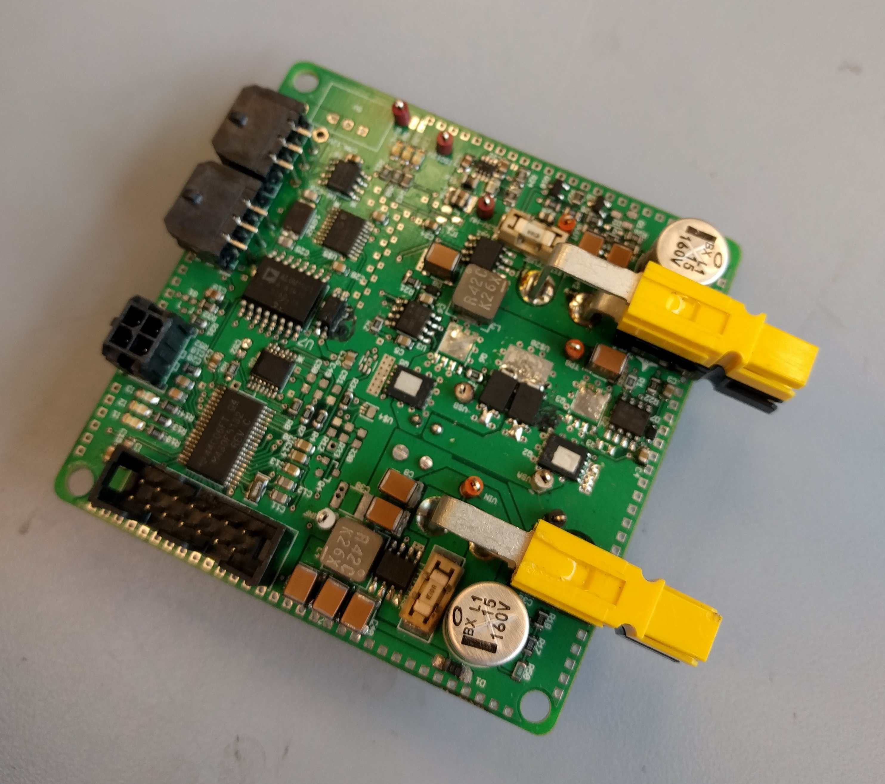
Version 2
Power Stage Design
The core of the MPPT is a two phase hard switched boost converter in continuous conduction mode (CCM). As with any boost converter, the MOSFETS charge up the inductors on the first part of the cycle, and then dump some of their stored energy into the output through an output diode during the second part of the cycle. A two phase design was selected because it reduces the ripple current requirements of the input and output filter. With each half stage running at 100kHz, the ripple current seen by the input and output filters is at 200kHz. Two smaller inductors are also easier to manage (and potentially have lower total losses due to skin and proximity effect) than one large inductor. Similarly, two MOSFETs each operating at half the total power are easier to heat sink than one large MOSFET.
Switches
The MOSFETS were selected to have low gate charge and low on resistance. There is a trade-off between gate charge and on resistance — the lower the one resistance for a particular semiconductor process and rated voltage, the higher the gate charge. Gate charge is partially responsible for and generally proportional to switching losses which are constant for a given output voltage and switching frequency regardless of how much power the converter is putting out (so long as its enough to keep it in CCM). On resistance is responsible for conduction losses which are roughly proportional to the square of the current the FET is carrying (ripple current also contributes). The FET we used, IPP320N20N3, was the best compromise that could be found for our output power and voltage range.
Version 1.0 With SMD FETs
MOSFET on resistance has a positive temperature coefficient; the warmer a MOSFET gets, the higher its on resistance becomes. While the prototype converter (which used SMD MOSFETS that were heat sunk to the board) never got close to its maximum temperature ratings, the efficiency suffered as the FETs warmed up. With the changeover in the final design to TO-220 packaged FETs clamped to a plate heatsink, heat is no longer an issue. This reverse mounted transistor heatsinking scheme can occasionally be found in commercial products like the iCharger series of lithium ion battery chargers.
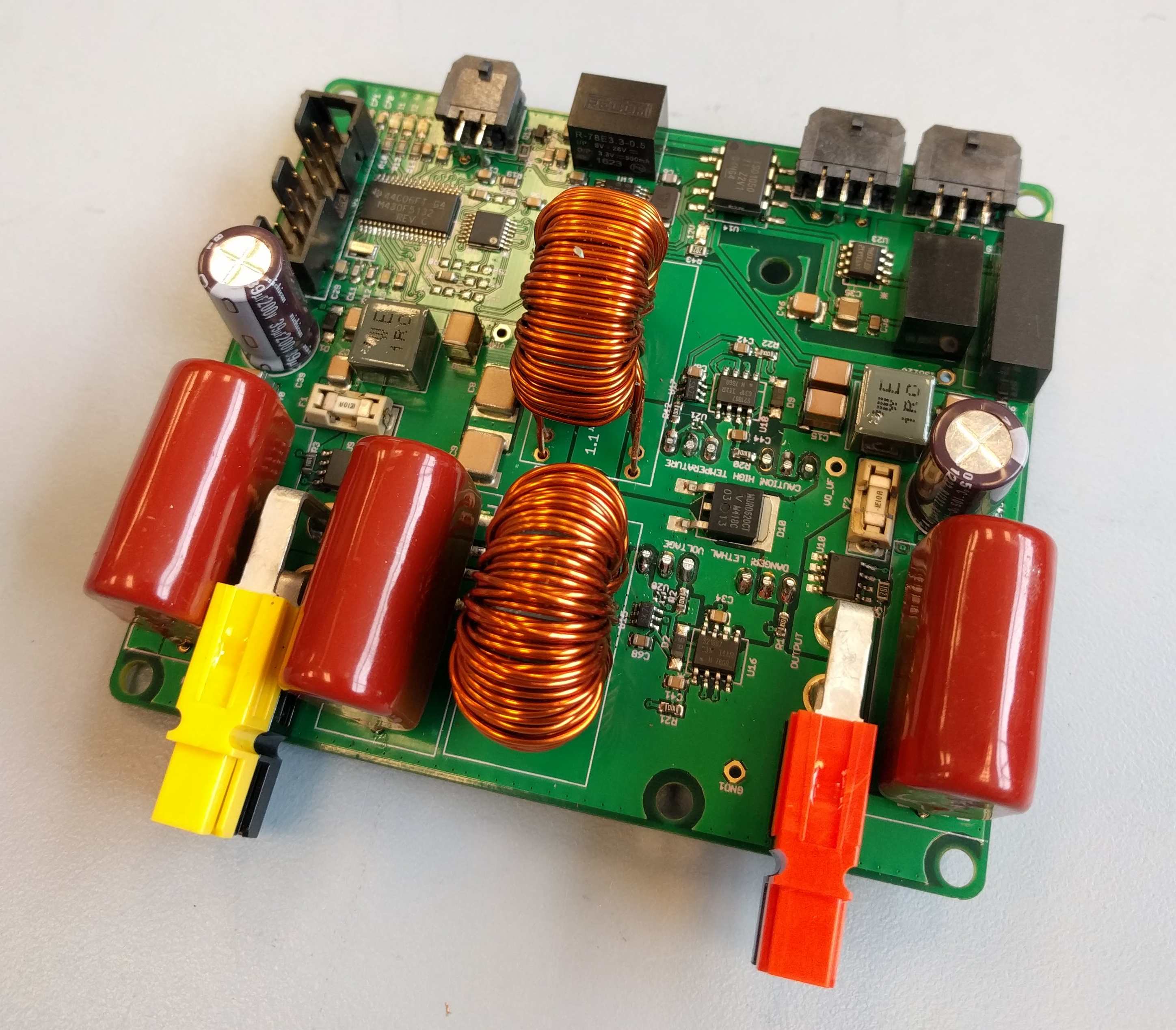
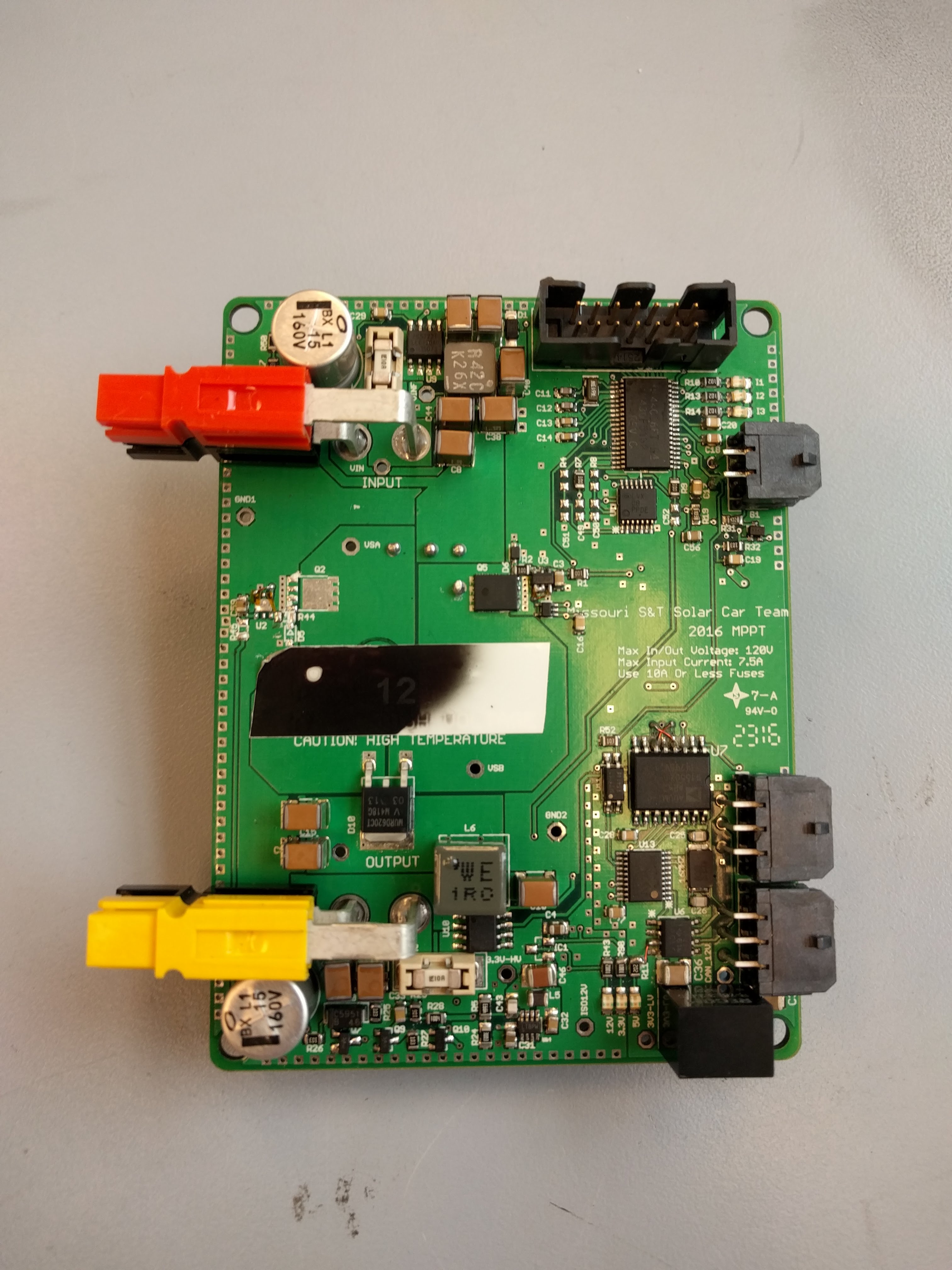
Placement of FETs on Version 2 Board. Synchronous Rectifier FETs Installed
Since designing this board, I have learned how effectively you can sink heat through a PCB using thermal vias. An equally good board using surface mount MOSFETs could be built with a section of the bottom of the board left bare of soldermask. An adhesive heatsink would then be attached to this section of the bottom of the board. I have successfully used this method in high power (500W) driver boards for wireless power transfer systems.
Diodes
The output diode is an ultrafast diode. This is important because standard speed diodes used to rectify 60Hz will not turn off quickly enough to prevent reverse conduction and will waste significant amounts of energy. A common cathode single package diode is used here so that both diodes stay around the same temperature. Experiments showed a nasty thermal runaway phenomenon where one half of the power stage would begin to carry a majority of the current because its diode was warmer (lower forward voltage drop). By using a dual package, the temperature of both devices can be kept the same.
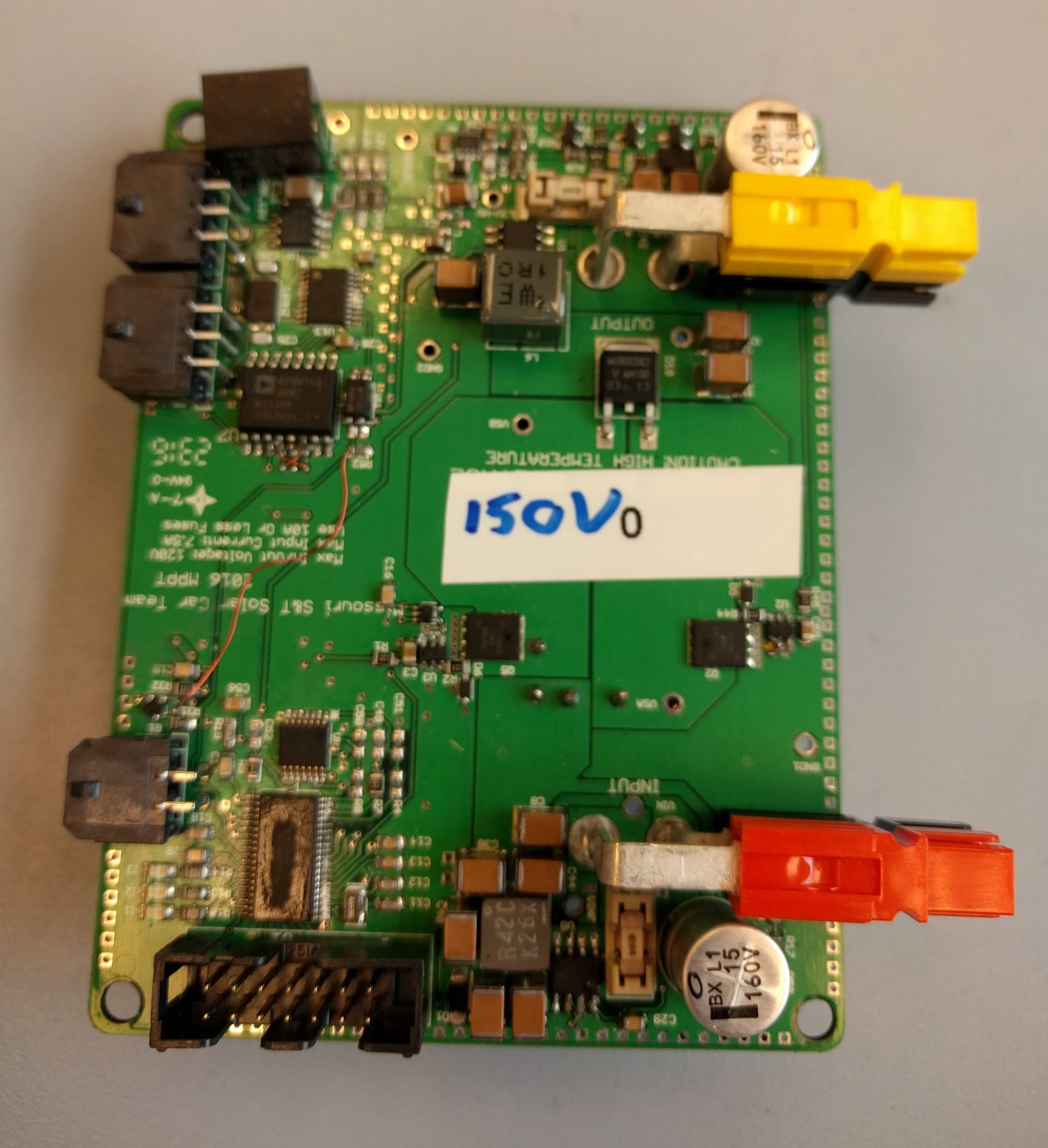
Version 0.2 Test Board Using Separate Diodes
The output diode is paralleled with synchronous rectifier FETs so that the ~0.8V diode voltage drop can be negated. Under most conditions, the synchronous rectifier FETs consume more power than the rectifier diodes due to switching losses. Footprints for a half bridge driver and the synchronous rectified FETs were still included in the final design since it doesn’t cost any extra to have a few more pads and traces on a board and it allows for flexibility in future experiments.
Magnetics
The inductors used in this converter use Magnetics Incorporated Molypermalloy Powder (MPP) Cores. These cores have some of the lowest possible losses, but they are more expensive than most other options. Total inductor loss is the sum of core and winding loss. Core loss increases with lower turns and copper loss increases with the number of turns. For this reason, at a given switching frequency, input voltage, input current, and duty cycle there is an ideal number of wire turns for a given core.
Core loss is a complicated term, but in general the larger the change in core flux per cycle and the higher peak core flux the higher the core losses. Peak core flux is dependent on the number of winding turns (increasing with increasing turns) and the change in flux is dependent on the inductance which is also dependent on the number of turns (change in flux goes down as turns increase).
Copper loss is dependent on the thickness of the wire which is constrained by the window area of the core, the maximum allowable fill factor, and the number of turns.
There are many ways of approximating the number of turns, but given that the manufacturer of this core provides equations for core loss (with polynomial turns up to the 5th power), it makes sense to instead write a script to automatically determine the ideal number of turns. I ended up writing a MATLAB script that simultaneously compared the performance of different MPP cores for the given operating characteristics of a converter. In general, larger cores allow for lower total losses, but the returns diminish after a certain point and larger cores cost and weigh more as well as require more copper.
Placement of Inductors on Version 1 Board
We ultimately decided on the C055351 core with a 70 turn winding composed of two 20 AWG wires in parallel. This yielded a 250 uH inductor with a resistance of 50mOhm. The total core and copper loss for both inductors was around 1.1W at the design input current (5.5A). Each of these inductors was hand wound using Polyimide insulated magnet wire.
Filtering
A C-L-C pi filter is used to smooth the current at the input and at the output. If substantial current ripple is present at the input, the solar panel will not be able to operate exactly at its MPP over the course of a switching cycle. A second order filter such as this one allows for much smaller capacitors and inductors to be used to achieve the same filtering. The converter operates at 100kHz, but the addition of a second phase explained in the next section increases the effective frequency seen by the filter to 200 kHz. After the DC bias effect on the capacitors is taken into account, the effective model of the filter becomes 10uF-1uH-10uF. The ESR of the electrolytic cap is around three orders of magnitude higher than the ceramic capacitors, so it has little effect on the cutoff frequency of this filter, but it does act to reduce the Q of the filter which reduces ringing at the resonant frequency of the filter and reduces inrush voltage spikes when the panel is first connected. This filter reduces current ripple at the input by around 30dB. Because the converter is in continuous conduction mode, the unfiltered input ripple is only ~0.5A. With the addition of this filter the ripple brought down to ~1mA.
Large ceramic capacitors are susceptible to cracking under even mild board flexure to the extent that NASA imposes size limitations for non-leaded capacitors. J-leaded stacked capacitors are used in this converter because the leads absorb flexing and protect the capacitors from cracking. The leads also allow for more capacitance in a smaller land area.
The reverse biased diode at the input to the converter is to protect against the solar panel being connected in reverse. While the current rating of the diode is not high enough to carry the full short circuit current of a panel continuously, it can carry the current long enough for the inductors to charge in reverse and allow the body diodes of the power stage MOSFETs to take the brunt of the reverse current. The converter is able to handle a reverse connected input indefinitely.
The output filter is similar to the input filter, but it has no film capacitor at its input. The higher bias voltage on the output capacitors reduces the effective circuit to 2uF-1uH-10uF which provides 28dB of attenuation at 200kHz. The ripple current is also higher than the input because the current falls to zero on every cycle. Assuming a 2.4A at the output of the power stage, the output of the converter will see a current ripple of around ~5mA. The inductance of the wiring to the battery and the battery itself will add at least 2uH of inductance which forms in effect a three stage filter with a 200kHz attenuation around 70dB, so the battery will not have much in the way of current ripple to deal with. The reason that no film capacitor was connected to the input of the output filter was that the LTSPICE simulations predicted that the parasitic inductance of this capacitor would cause some ringing problems that would actually make ripple current worse.
Isolated Power Supply
The isolated power supply chip works by chopping up the input 12V DC power, passing it through a transformer and rectifying it. The initial low profile chip introduced quite a bit of switching noise into the CAN bus network. I tried to low pass filter its inputs, but it did not have much effect. I realize now that I should have put a common mode filter on the input of the board. The larger through hold isolation module used on the second version of the board put far less noise on the CAN bus. An EMI reducing high voltage capacitor was also added between the power and isolated grounds which seems to have reduced noise as well. This board would likely fail an official FCC radiated emissions test, but it is a test board being produced in small quantities that isn’t being sold to anyone.
Protection
The maximum input and output voltage of this converter is limited by
the rating of the FETs in the power stage which is 200V max. The
converter should not be used at voltages greater than 160V in order to
maintain a margin of safety. The other components in the power stage are
rated to similar voltages:
– MOSFETs 200V
– Diode 200V
– Electrolytic Capacitor 200V
– Ceramic Capacitor 250V
The converter is designed for 5.5A, but it can handle up to 7.5A continuous without heating up to a degree that would require the heatsink to be re-evaluated.
Startup
I wanted to make sure that the Microcontroller was fully booted up before power was applied to the gate drivers, so I added a delay circuit made from two N-channel MOSFETs and a couple resistors and capacitors. It may or may not have been necessary, but was worth the extra dime in BOM cost. There is also a similar delay circuit on the boost enable circuit that enables passing the PWM signal to the gate drivers. This delay was added to ensure that the enable AND gate was never trying to feed into a gate driver that was off.
Overvoltage
To prevent the maximum operating voltage of the converter from being exceeded, I added a circuit to shut the converter down if the output voltage exceeds a particular value. It uses a 150V Zener diode to form a sort of comparator circuit the output of which is passed to an AND gate as the boost enable signal. When the output voltage exceeds the rating of the Zener diode plus two base to drain voltage drops, an NPN BJT sinks current from the enable line. In actual operation, the circuit works quite well. The converter never goes above the intended voltage, though interestingly the gate drivers start to consume more power since they are bouncing between on and off at many times the normal switching frequency as a result of the protection circuit having no hysteresis.
This circuit protects the converter against battery disconnections. In normal operation, when any cell in the battery reaches maximum voltage (4.2V) charging is disabled. This is accomplished by opening the battery charge contactor which means that the MPPTs suddenly have no load. Because of this circuit and the output electrolytic capacitor, the circuit is able remain at safe voltages when this happens.
This protection is pretty sloppy, but it gets the job done. Since it has no hysteresis, the gate driver is presented with random low duty cycle high frequency pulses when it is in overvoltage protection mode. The power consumption of the gate drivers increases, but now to an extent that will damage the board. Ideally, code on the microcontroller would detect an overvoltage condition and shut off the PWM outputs shortly after the analog protection circuitry kicked in.
If I were to make this circuit today, I would probably over complicate things and use an analog comparator with a feedback circuit to provide hysteresis to prevent the random narrow pulses from triggering the gate driver. As built, the circuit is functional and is a good example of how you can get away with using discrete parts in a lot of applications where an IC is typically used if you are careful.
Control
A TI MSP430 chip is used to control the MPPT. This chip was chosen because it has the ability to generate multiple phased PWM outputs with high precision. Since the PWM signal is generated digitally, the maximum frequency of this signal is normally limited by the clock frequency of the microcontroller and the bit resolution of the PWM. If you have an 8 MHz clock and 10 bits of PWM resolution, the maximum PWM frequency would normally be 62.5 kHz. This chip, however, includes an internal clock multiplier that is used to provide ‘high resolution’ PWM outputs.
The micro takes in analog readings from the input and output current sensors and from the input and output voltage dividers and uses them to determine the ideal duty cycle using a perturb and observe algorithm. The microcontroller also sends telemetry back to the car through a CANBUS interface. Other members of the team programmed the microcontroller and provided me with sketches of the circuits to implement for CAN communications.
Possible Improvements
A converter operating in discontinuous conduction mode (DCM) with bulkier inductors and switching components can theoretically attain higher efficiency than a converter in CCM because of the reduced switching losses which make synchronous rectification tenable. CCM was chosen because it reduces the ripple current requirements of the input and output filters and because it reduces MOSFET conduction losses and inductor core losses. At the expense of perhaps 1% absolute efficiency, this converter is able to be much smaller and lighter than other solar car MPPTs. Most importantly, it can be easily manufactured in house.
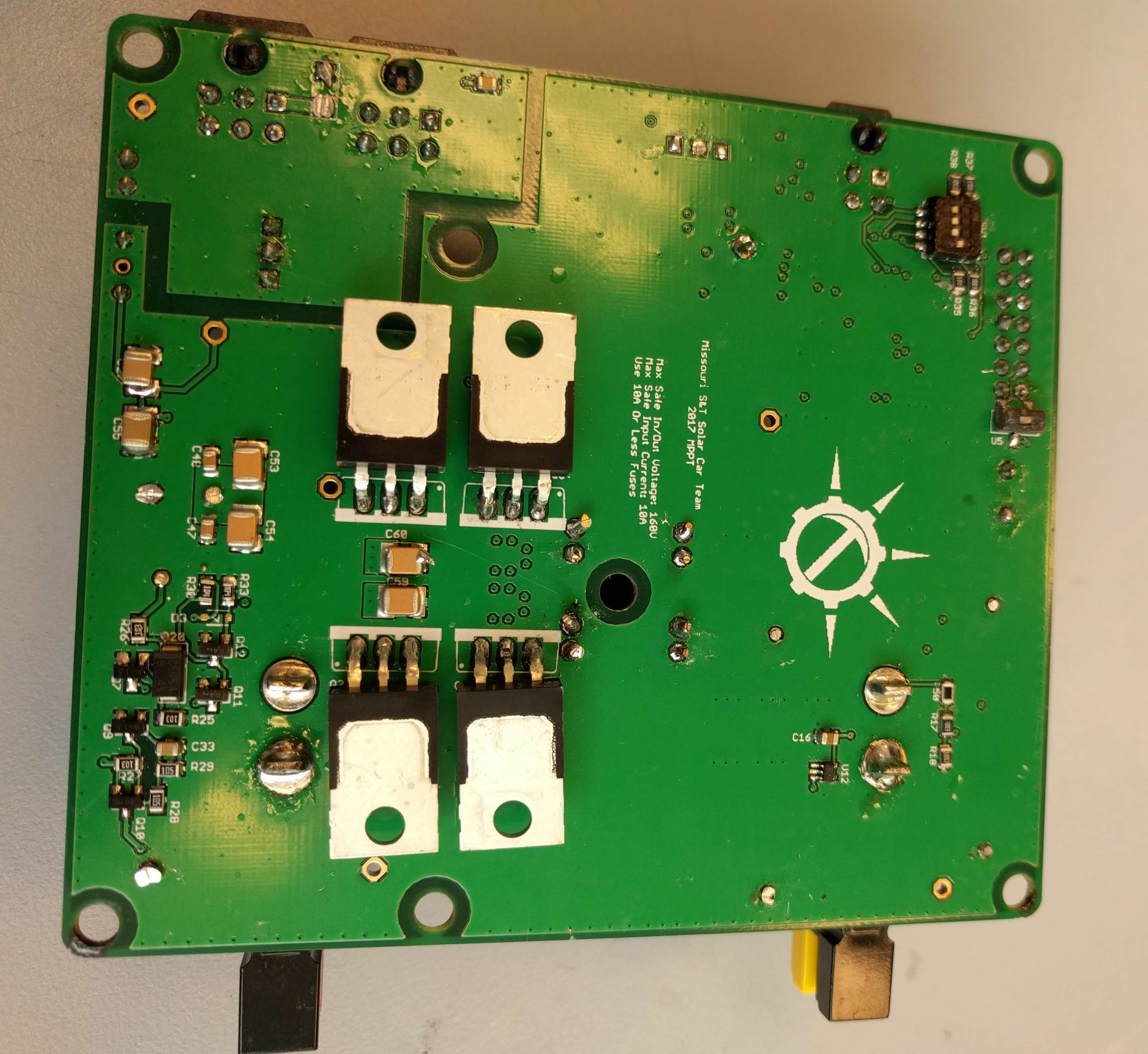
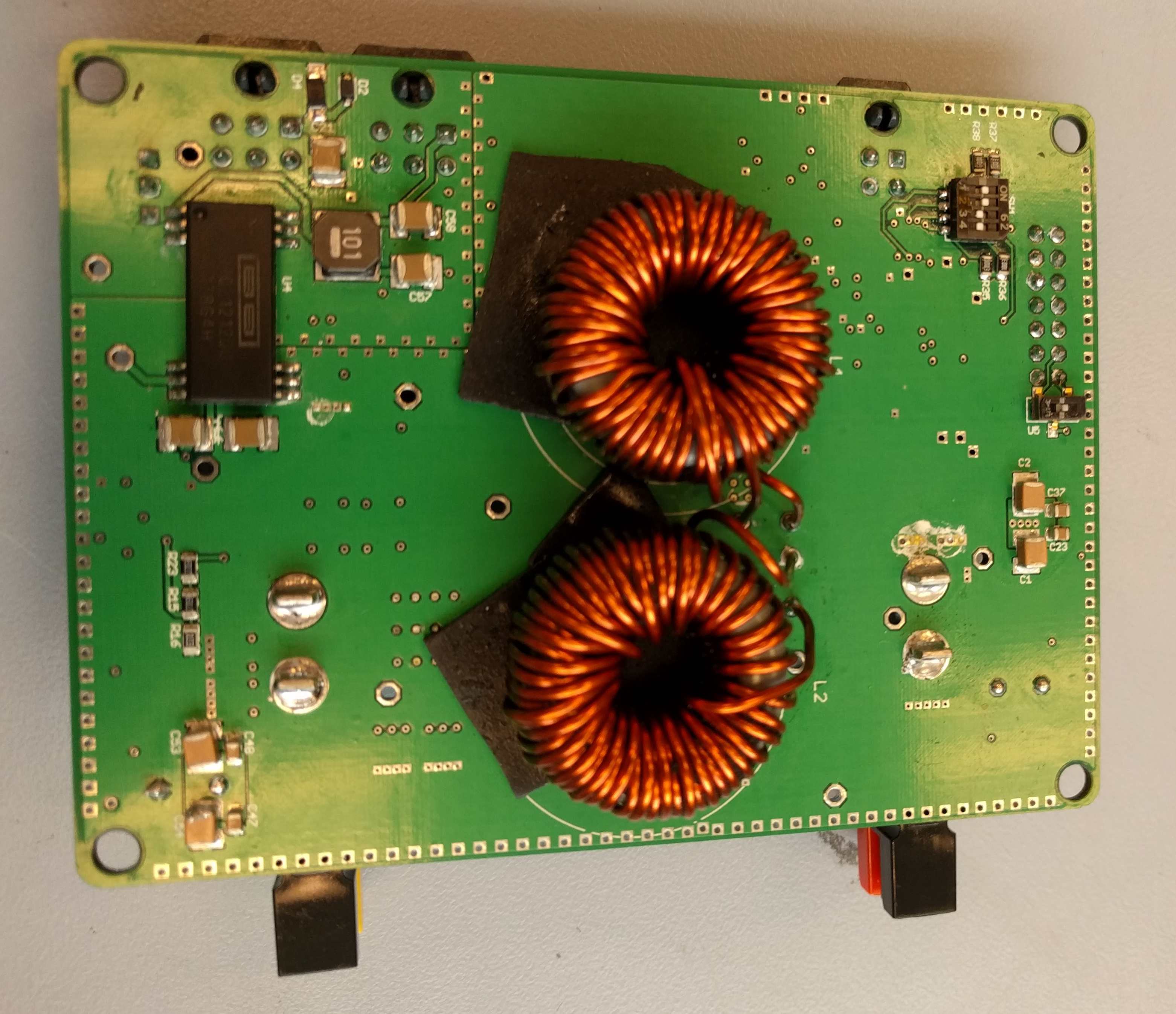
Additional Pictures
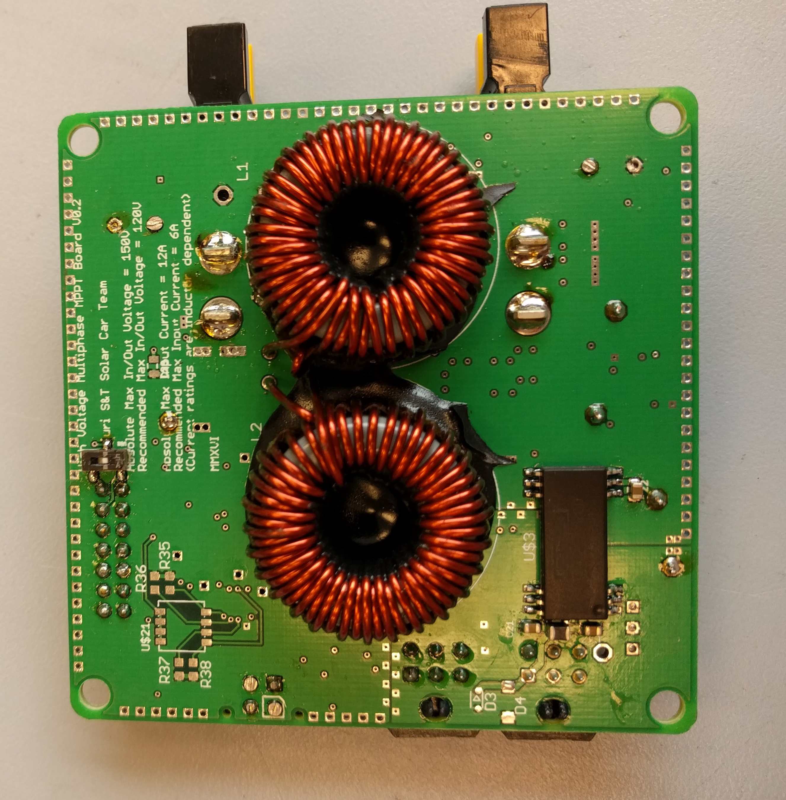
Version 0.2 Bottom
Version 1 Top
Version 1 Replacing Parts