DNVT Teardown
2023
The most common (and best looking) DNVT available is the TA-1042A/U. Other compatible units include TA-1032 and TA-954 which are, by comparison, bulky, ugly, and cheap feeling. CA-67 is an AC powered variant that also appears to be compatible, but I have not tested it out. I took these phones apart in order to design a switch interface for them — I could have treated them as a black box and come up with a functional interface, but I wanted to make sure that I wasn't missing anything and that whatever I built would pose no danger ot the phones. Unsurprisingly, the phones are quite electrically rugged, and it would be difficult to damage them unintentionally. I based my interface circuitry off of what I found inside the TA-1042 as detailed below.
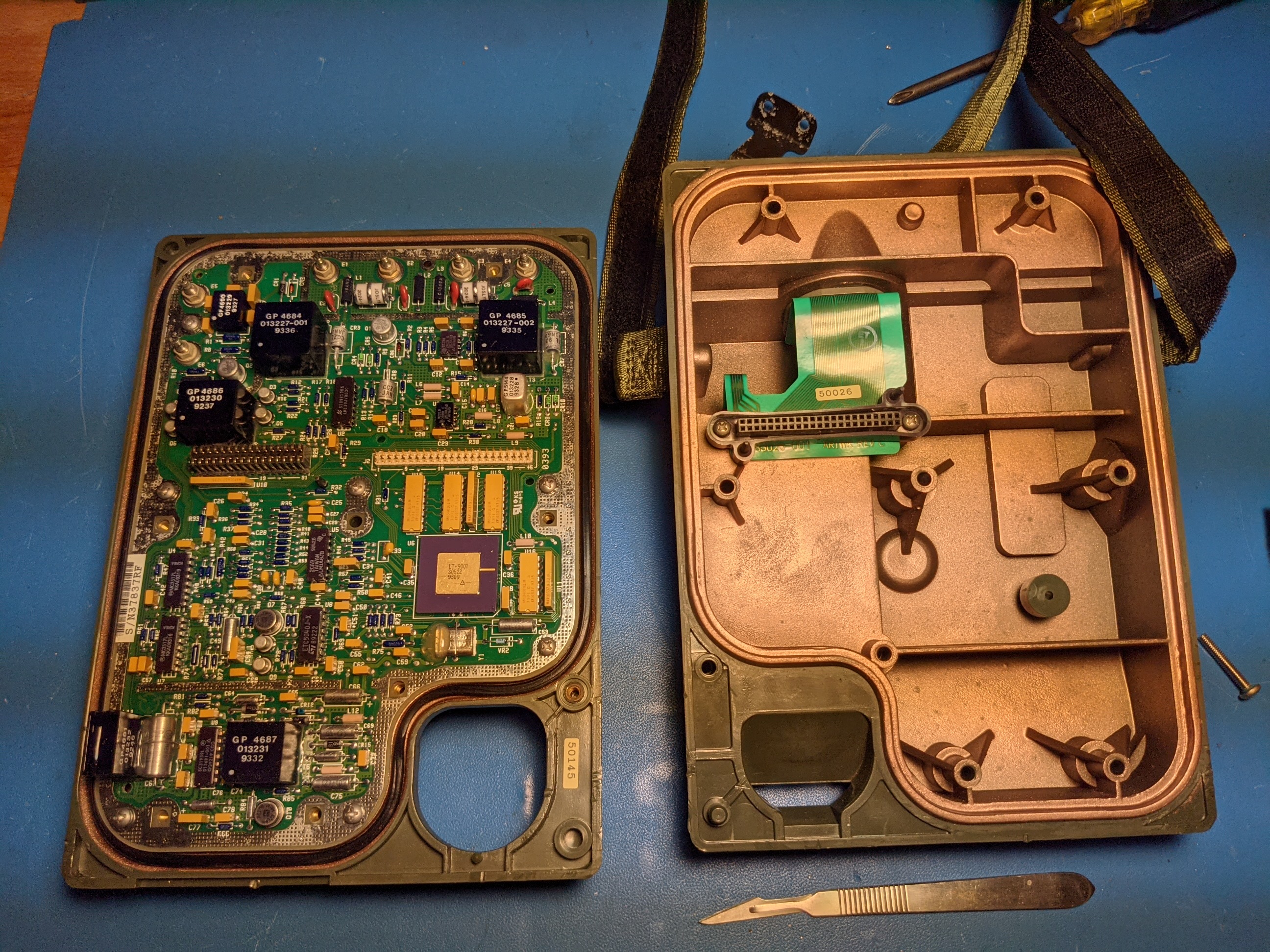
TA-1042 Opened Up
TA-1042
There are already good pictures of the insides of TA-1042 on the RadioNerds website courtesy of Mark Blair, so I will focus on what's going on on its circuit board. The phone is packaged quite nicely. The PCB interfaces with connectors for the data port and number pad with blind mate connectors that self-align with guide pins when you close the cover of the phone. The inside of the case is metalized for shielding, and the whole assembly is sealed together with a rubber gasket. The operating manual for these phones specifies that they are design for use in tents and shelters on desks as well as outside strapped to posts and trees.
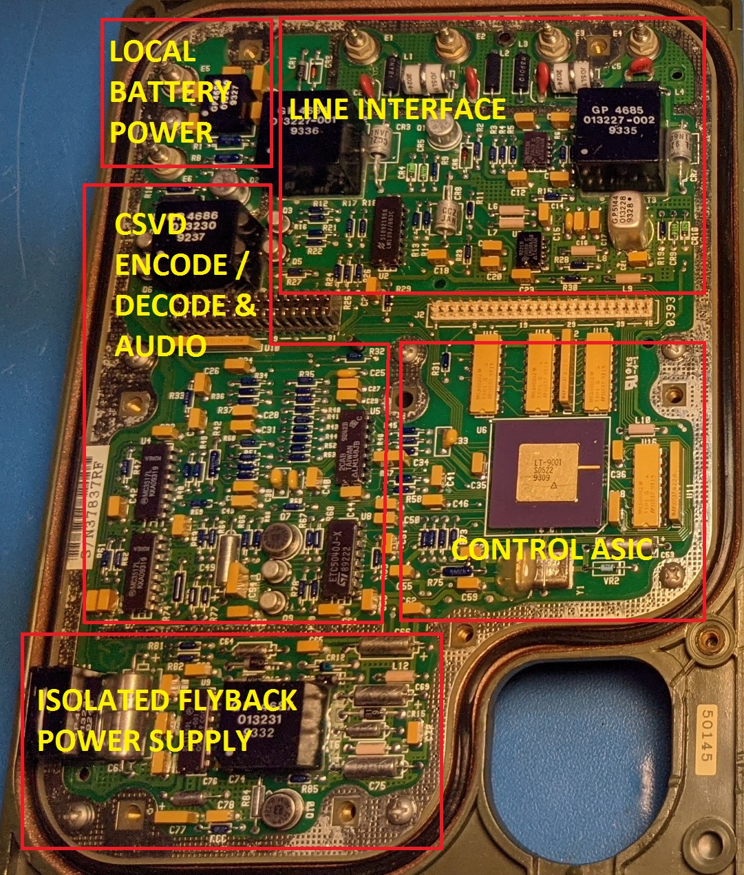
TA-1042 PCB Annotated
The circuit can be broken down into a few sections. I sketched out the circuitry for the line interface, flyback supply, and local battery power sections only. Since I was initially only interested in controlling the phones, I skipped the audio section. Ultimately, we ended up decoding and encoding CVSD audio in software, so there was no need to reverse engineer the filter constants, etc. for the CVSD chips.
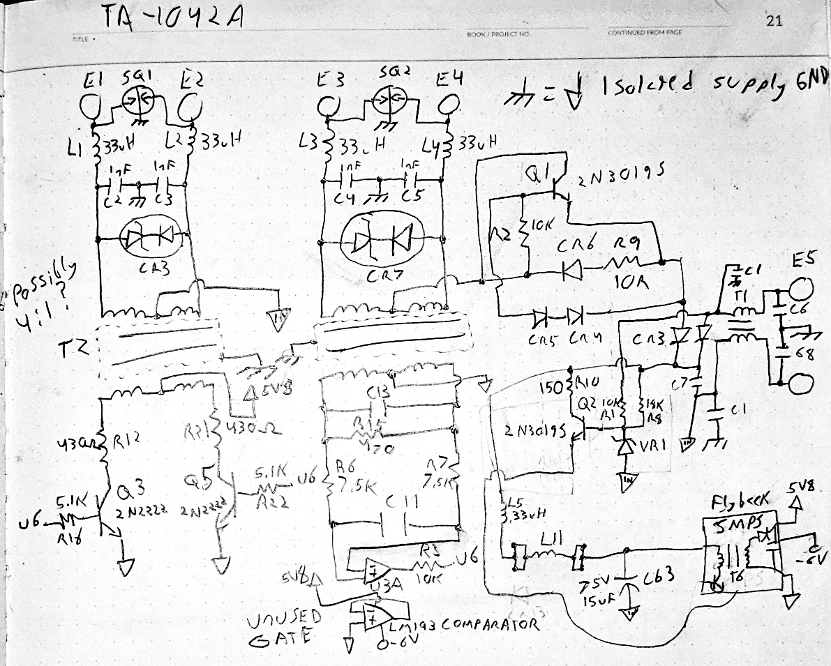
Line Interface, Flyback Supply, and Local battery Power Input Section of TA-1042
Line Interface
DNVTs run power and data over their XMT and RCV pairs. The data is superimposed on a DC common mode voltage. This common mode voltage is taken from the center taps of the custom transformers to power the phones. I cover the specifics of this as well as the input protection circuitry on the Physical Interface page. The data transformers are custom wound parts.
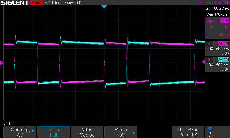
Measured Output of DNVT into 100Ω Load
The transmit transformer is driven push-pull with 5.8V applied by the phone to the center tap of its primary windings. The low side NPN transistors are driven directly from the large control ASIC. Comparing the measued output voltage when terminated by a 100 ohm resistor to an LTSPICE simulation reveals that the transformer is has a 2:1 (not a 4:1 as a scribbled in my notebook) turns ratio. Each half-winding on the primary side has a 1:1 turns ratio with the secondary (output) side, the sum of the two primary half-windings makes it a 1:1 transformer.
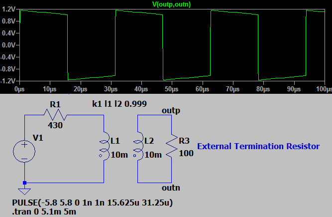
Simulation of TA-1042 Transmit Section
I did not measure the output of the receive transformer, but given that the termination resistor is 470Ω and these phones are designed for use with 120Ω wire, its reasonable to assume that the receiver transformer has a 1:4 winding. The center tap of this transformer is connected to the isolated ground of the phones to provide a DC level to the received signal. The differential signal from the line is received by a LM139 comparator. The output of this comparator runs directly to the control ASIC.
Power
The phones can be powered either off of their local battery (LB) posts or in common battery (CB) mode through the XMT / RCV lines. The phone doesn't care how it is powered. You can use it in CB mode with no voltage on the XMT/RCV lines and apply power through the LB posts. Conversely, you can use the phone in LB mode talking to another phone if you couple power onto the RCV/XMT lines. I was able to test this by taking two interface boxes that I built and cross-strapping their receive and transmit lines. When using the phones in LB mode, both phones need to be separately powered — the phones do not apply power ot the lines.
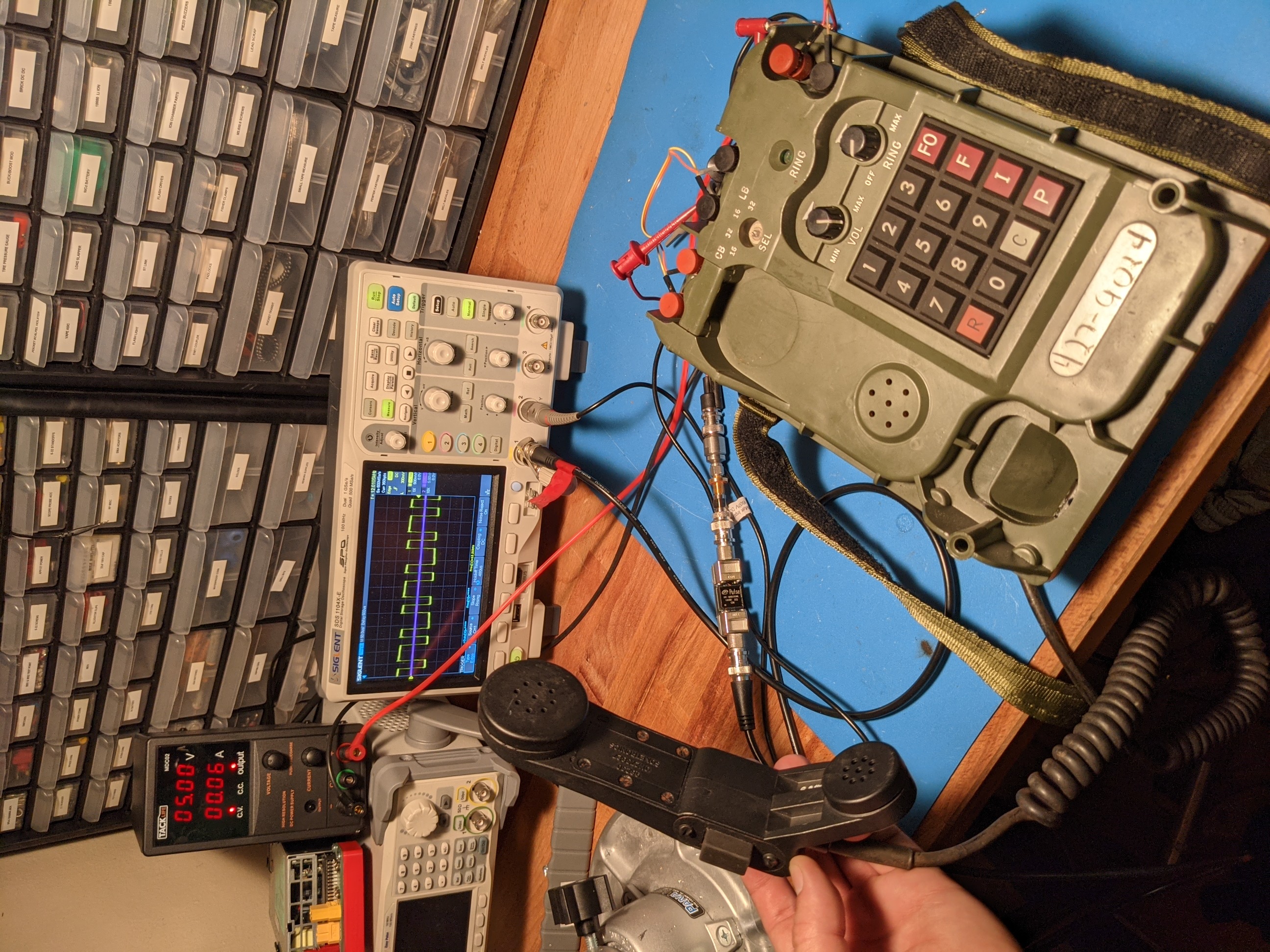
XMT of LB Powered Phone Observed on a Scope through an Isolation Transformer
The phones have different voltage requirements depending on how they are powered. You can run a phone off of 12V when powered through the LB terminals, but a phone requires at least 20V when powered CB style. There is an extra series circuit (shown in the schematic) present between the transformer center tap and the SMPS input that (I guess) likely provides additional transient protection and but requires more voltage headroom. Both the CB and LB inputs are reverse voltage protected, so you don't need to worry about mixing up the polarity of the phones. The LB input passes through a common mode choke before dumping into the same input filter as the CB circuitry.
The power supply appears to be a typical low side switch isolated flyback design. I didn't investigate it too closely aside from determining the board's grounding. Many components, such as the receive comparator, have both positive and negative power supplies. Both of these are supplied by the flyback. The ground of the flyback output is connected to chassis ground, so while I drew both board ground and chassis ground symbols on my schematic, the two are actually connected. It is only the power input section that has an isolated ground which I marked with "IN" inscribed in a board ground symbol.
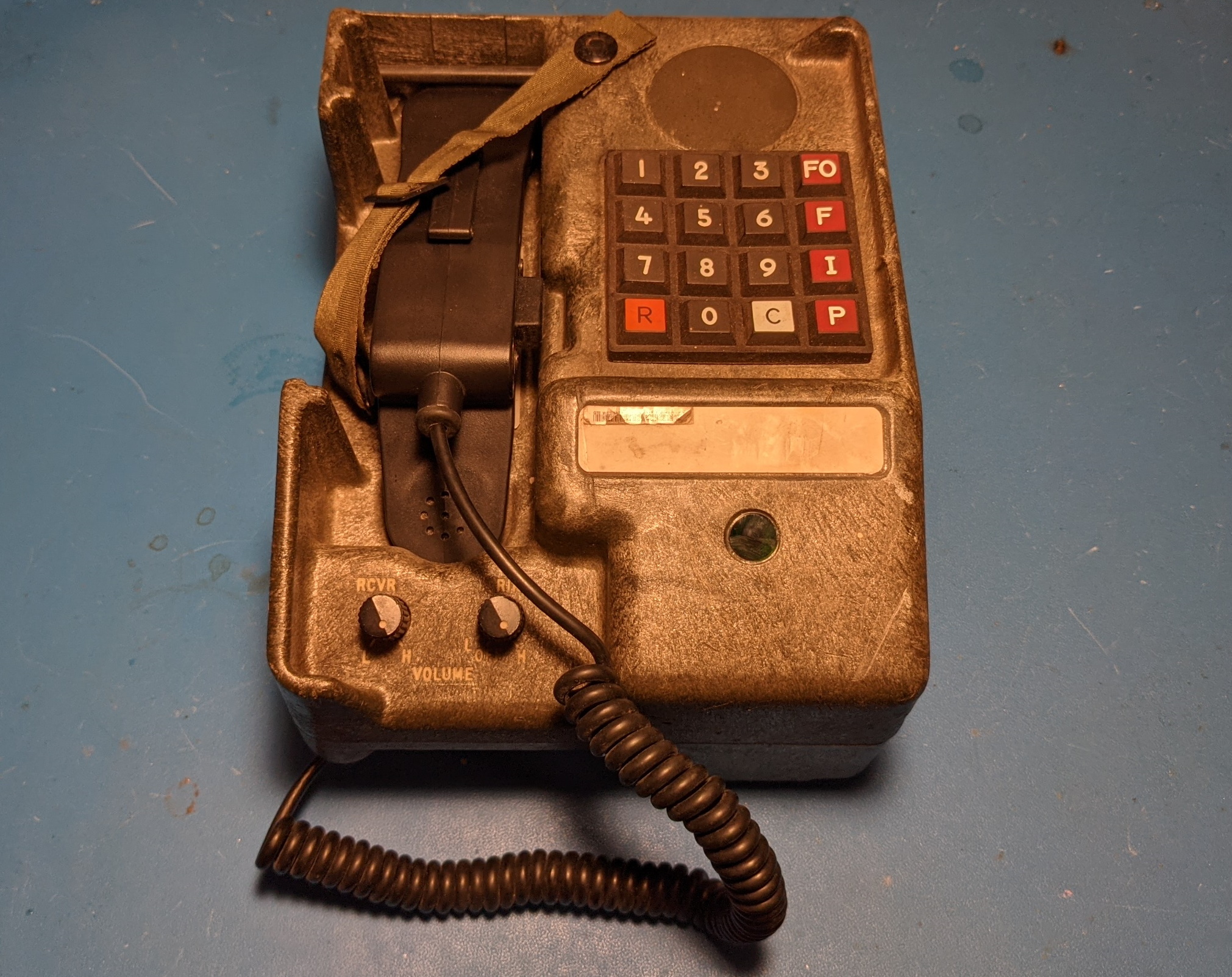
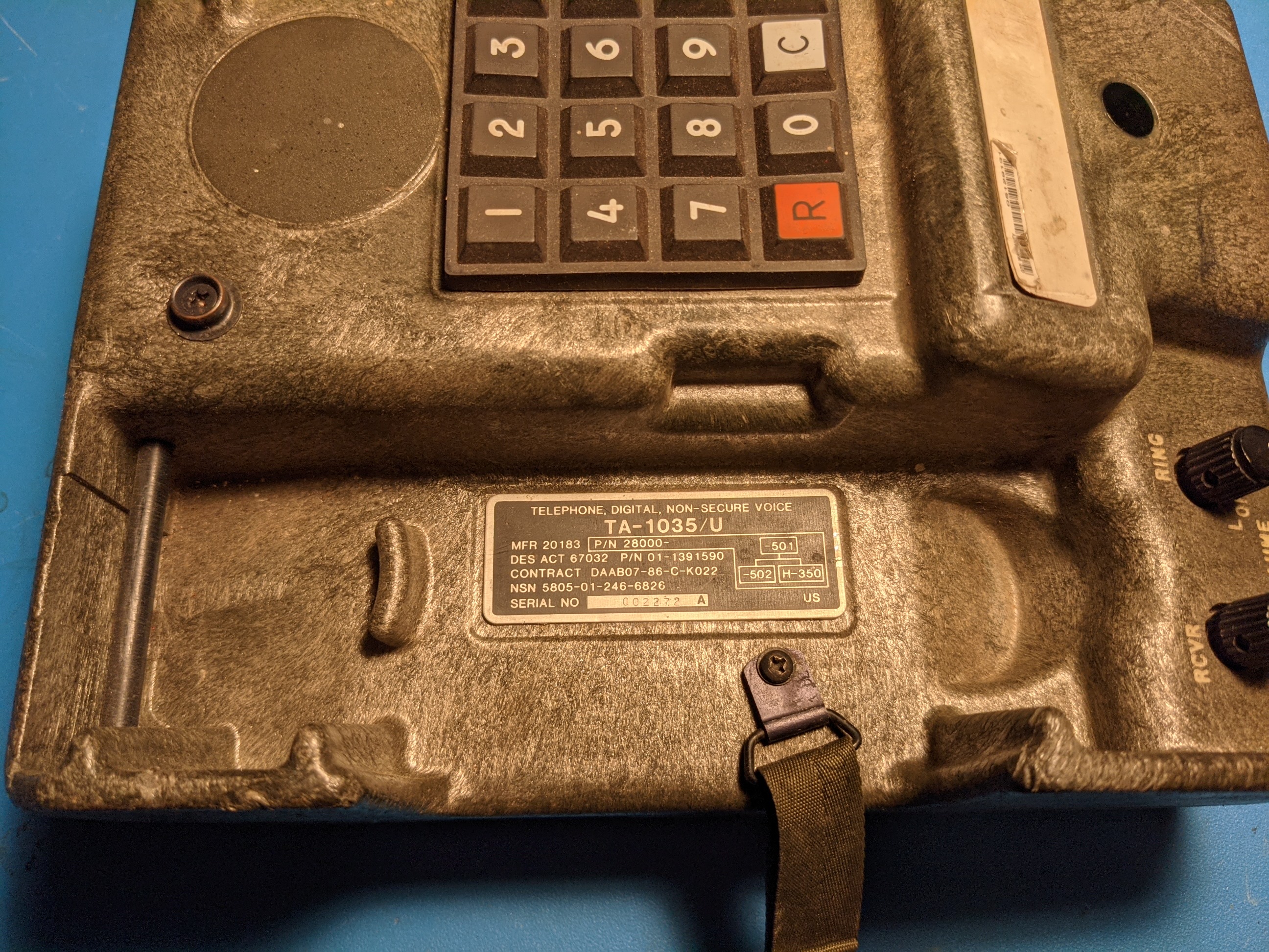
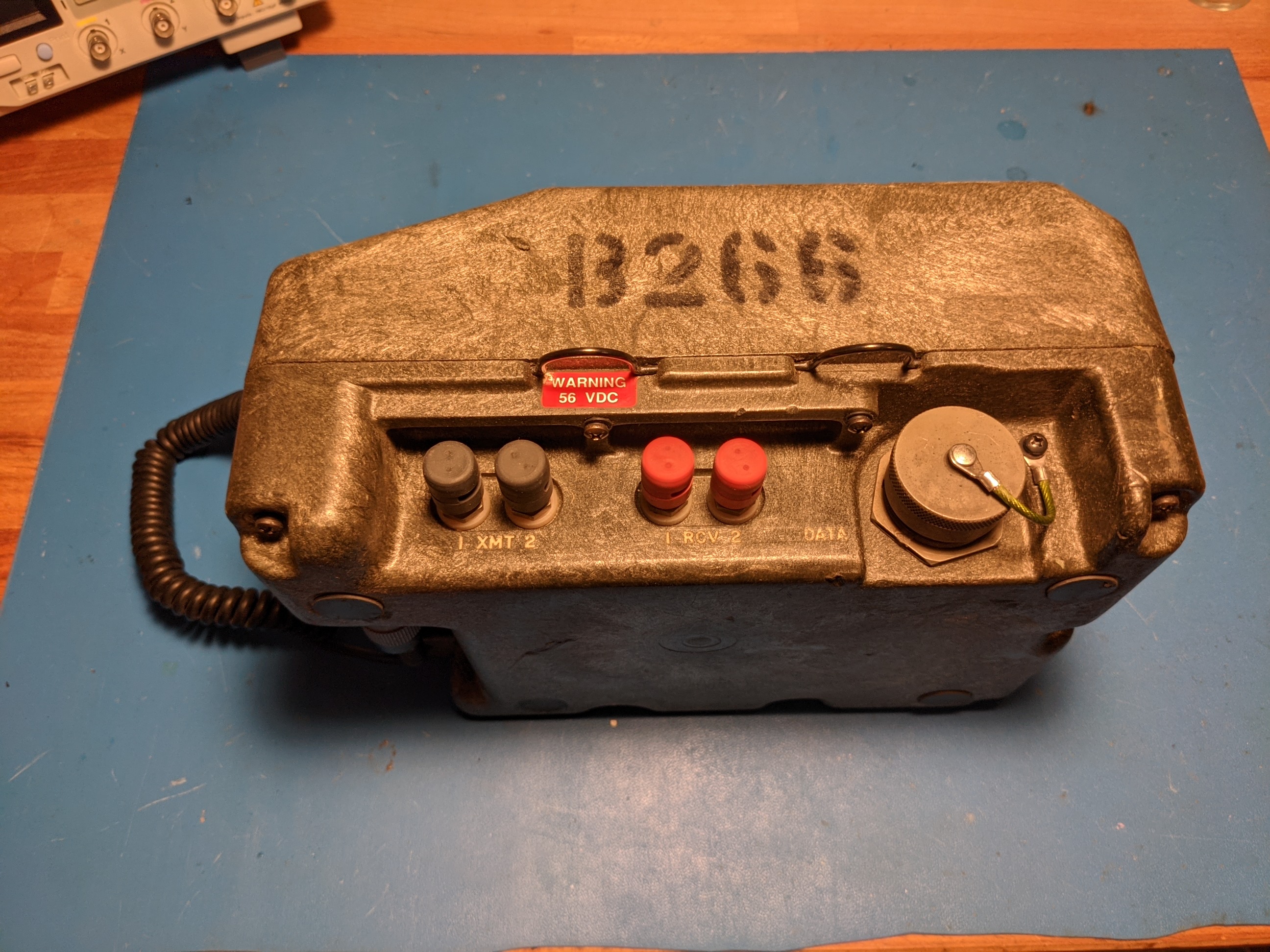
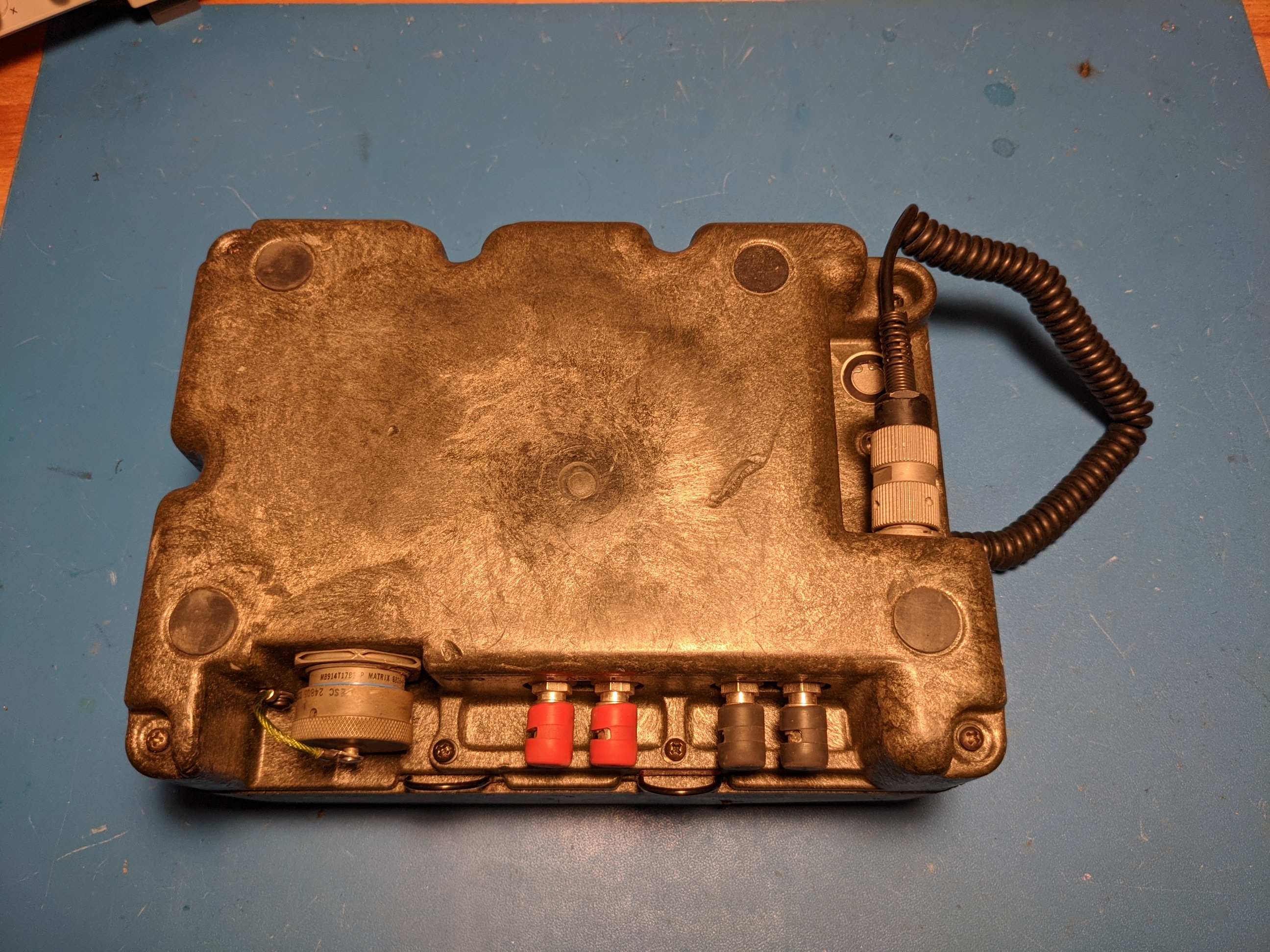
TA-1035
I bought a TA-954 off of ebay, but I received a TA-1035 instead. The differentiating feature, aside from the clear label under the handset that did not match the picture of the phone in the listing, between the phones is that TA-954 is adjustable rate (16 kbps or 32kbps) while TA-1035 is fixed rate (mine is 16 kHz). In the place of a rate selection knob, TA-1035 has a data port to connect fax machines. The TA-1035 that I received also appears to have a handset or audio problem, but I confirmed that it otherwise works with the switch (dials and rings). Nick bought functional examples of both TA-1035 and TA-954, so I can confirm that they do work with the switch.
TA-1035 uses a different control ASIC, transformers, and general construction method than TA-1042, but it uses the same CVSD chips (MC3517).
TA-1035 DNVT
TA-1035 DNVT Cradle
TA-1035 DNVT Side
TA-1035 DNVT Bottom
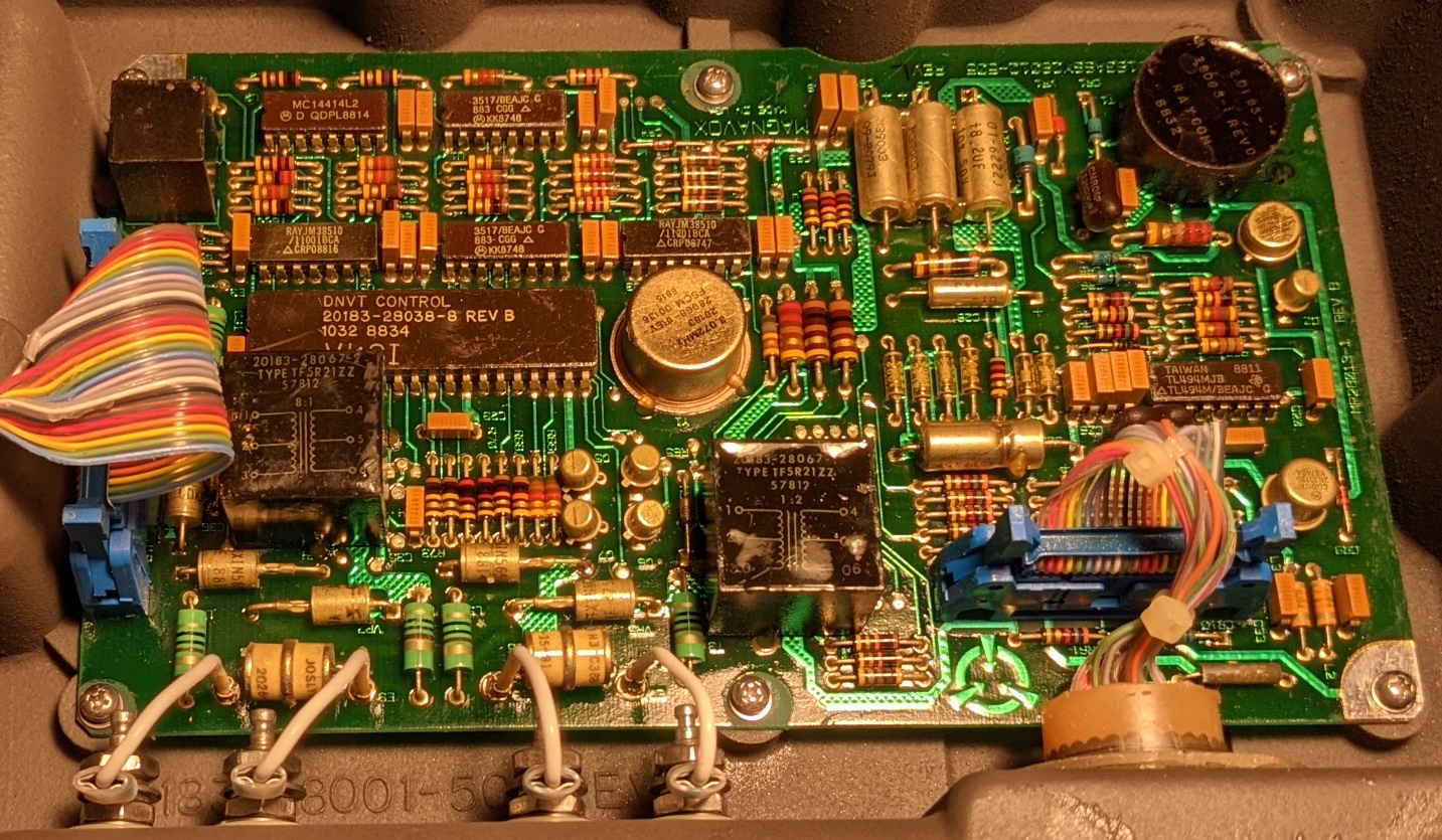
TA-1035 DNVT PCB