Pure Sine Wave Inverter
2019
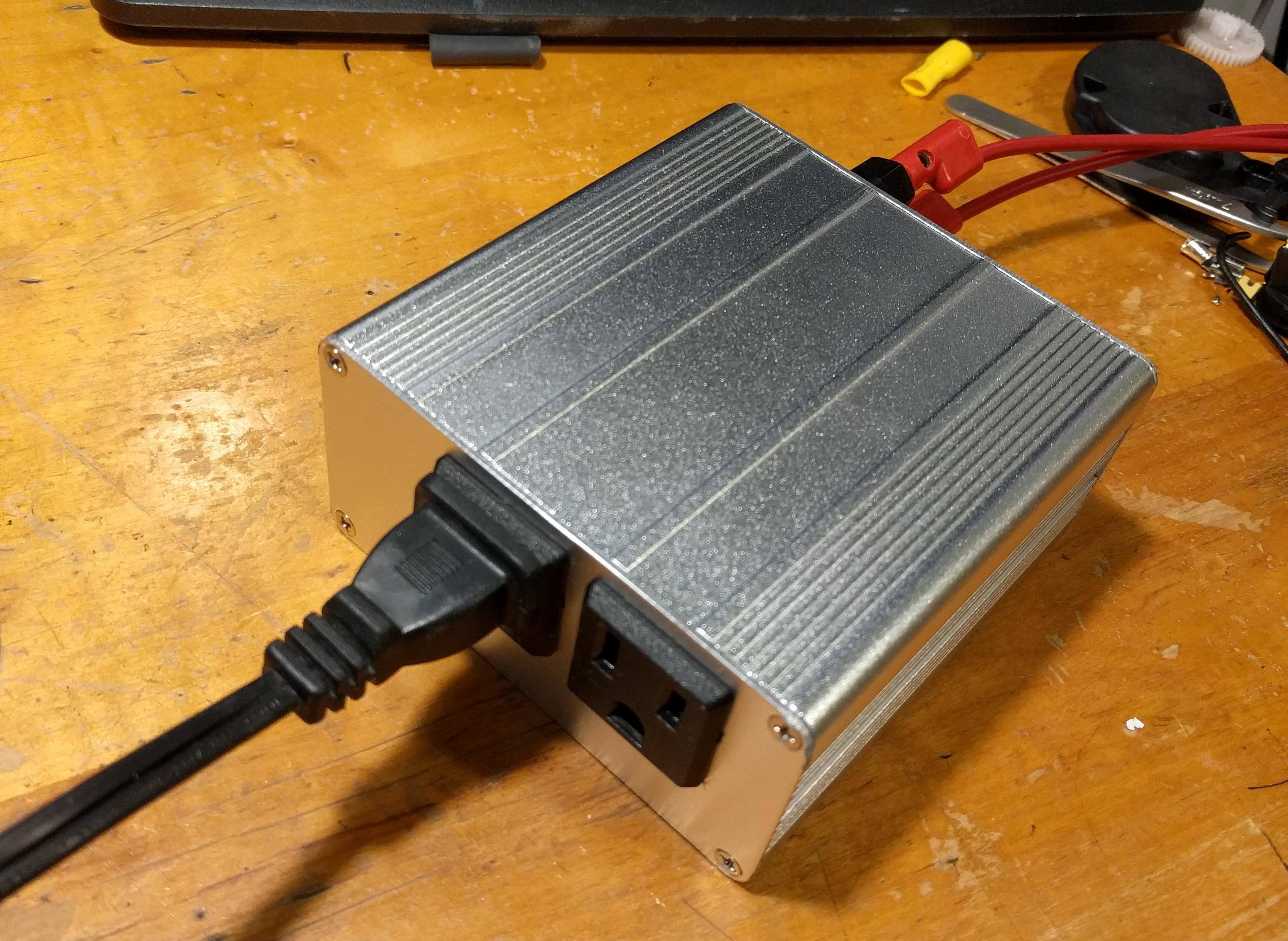
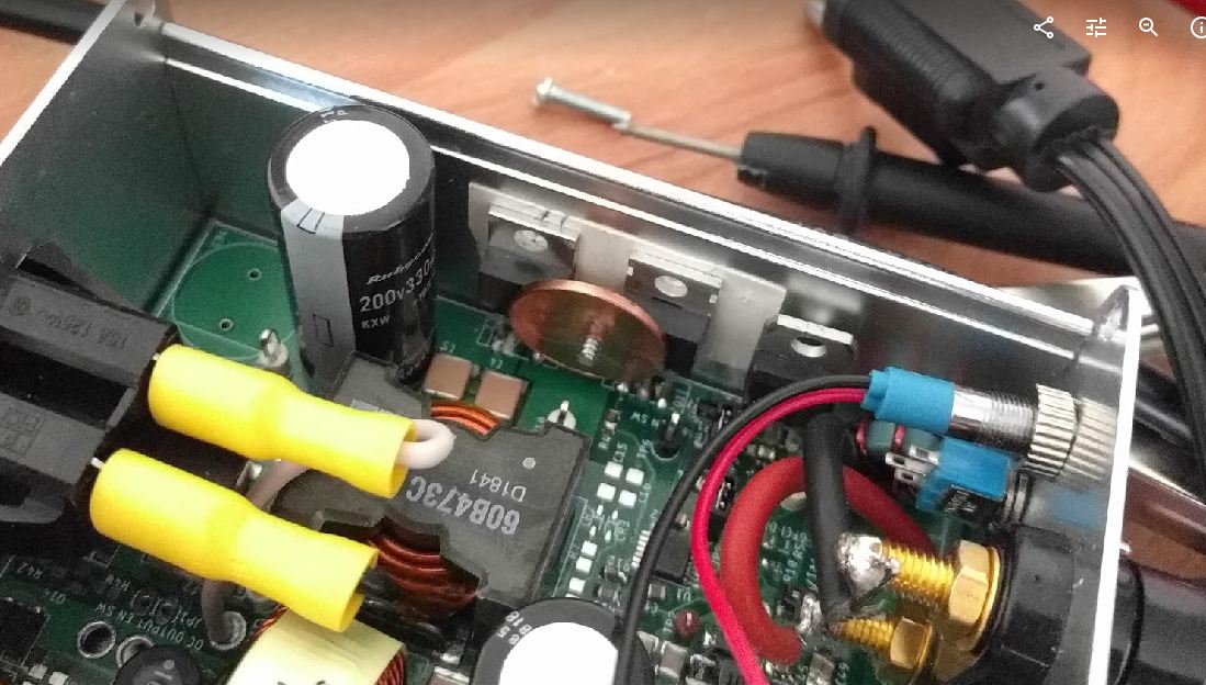
Most commercial power inverters have relatively limited input voltage ranges. I wanted an inverter that could provide 150W of output power with an input voltage range of 12-100V for use with custom lithium battery packs, so I decided to build my own.
Early Test
Schematic
Layout
EagleCAD Files
Background
This being a pure sine wave inverter was actually an afterthought. My main goal was to build a converter that gave me a 170Vdc output to power devices with switched mode power supplies. Pretty much anything with a modern power brick is happy to run off of a DC input since the first stage of all of these converters is either a diode rectifier or a power factor correcting boost converter. Devices that have capacitive dropers or voltage doublers will not work off of a 170V DC input, devices that have transformers will probably blow a fuse, and devices that are resistive will consume as much as twice their normal rated power. I realized I had enough room left on the board to suport the circuitry needed to take this 170V DC output and convert it to a 'pure' sine wave, so I added that in at the last minute.
There is a huge amount of bad information on the internet about DC to AC power inverters. If you try to look up schematics for power inverters, pretty much everything you find would never be used in practice. The only decent information I have found on power inverter design is in a few application notes. I also tore down a cheap 12V to 120VAC power inverter and looked inside a friend's 48V pure sine inverter to see how they were designed.
Theory
Power inverters are composed of two power stages. The first boosts the input voltage up to the peak voltage of the output sine wave plus a margin. A 120Vrms output requires 120*sqrt(2)=~170Vdc in order to generate the the full range of the sine wave. The second stage of the power inverter uses a full bridge to chop up the 170V into a pulse width modulated output. This output is not a sine wave because power electronics are only efficient when they are hard on and hard off. That is to say that the output of the full bridge is ideally at any instant is either +/-170V or 0V. To get an actual sine wave from this output, the signal needs to be low pass filtered using an LC circuit.
The control signals are shown below. One half of the bridge generates the 'positive' side of the sine wave, and the other half of the bridge generates the 'negative' half of the sine wave. HA and LA are compliments with dead time (time between transitions when both are low) as are HB and LB.
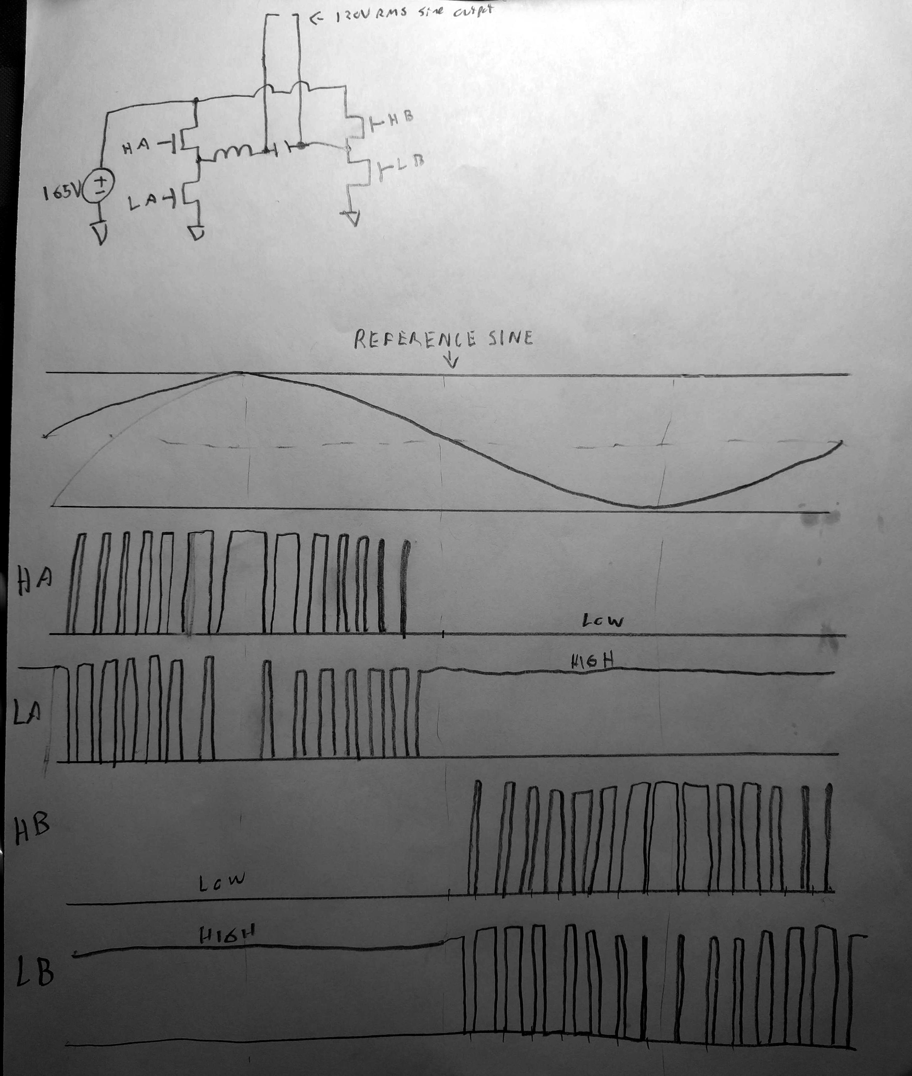
Sketch of Control Signals
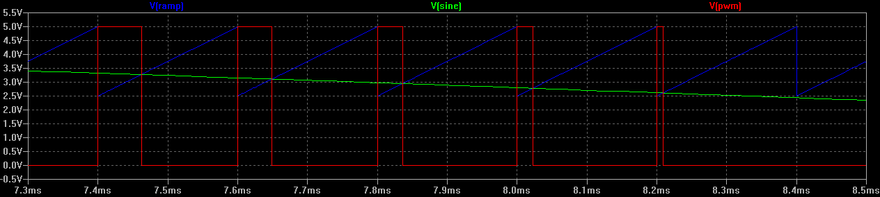
PWM signals that drive the full bridge are generated by comparing a reference sine wave at the desired output frequency to a sawtooth or triange wave at the desired switching frequency. This can be done using analog circuitry, but these days it is far easier to use a fast microcontroller. One register counts up, and when it passes the reference value, it turns on output on or off.
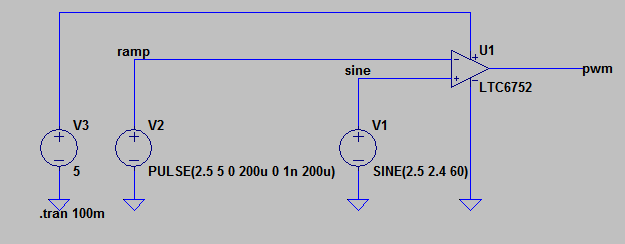
Schematic of Comparator Based PWM Generator
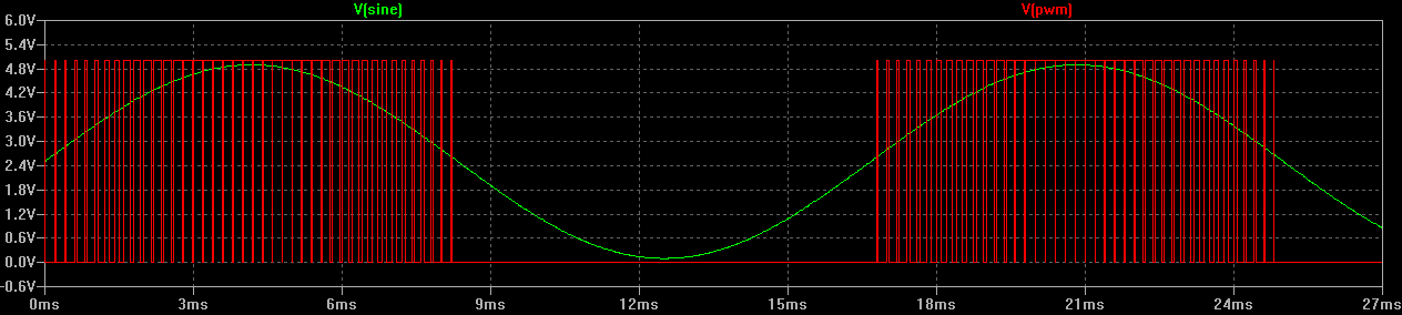
Simulation Output
Here, the ramp is offset by half the amplitude of the reference sine so that the active is only active on one half of the cycle.
Simulation Output with Ramp
The swiching frequency in this simulation is 5kHz which was chosen so that the changes in duty cycle as the reference changed are noticeable. When the reference exceeds the ramp, the output goes high.
The high side of the first half bridge can, alternatively, share a control line with the low side of the second half bridge, but driving like this has greater output ripple. The benefit of this method is that it is easier to implement in analog while still ensuring that the output does not have a DC bias.
Modified Sine Wave Inverters
Modified sine wave inverters approximate a sine wave by producing a three level output. This has the benefit of reducing switching losses on the full bridge and eliminating the cost of the output filter. The downside is that the output waveform has a lot of harmonics which mostly just causes issues with devices that have motors or transformers. Transformers will buzz at the harmonics of 120 Hz.
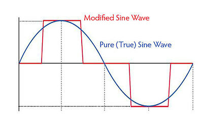
Modified Sine Wave
My Design
My design relies on the boost stage regulating the output voltage unlike most commercial converters which have variable intermediate bus voltages and adjustable duty cycles in the final inverter to compensate. The benefit of regulating in the final stage is that a more efficient fixed ratio boost stage can be used, but it comes at the cost of limiting the range of input voltages.
Input
I added a simple LC filter to the input to limit the differential mode conducted noise, and I added enough input capacitance to make the converter insensitve to the inductance of the wires to the battery. I then fused the input to protect the battery against a short circuit failure in the converter and added an inrush limiter that also acts as a on-off switch. Without an inrush limiter and assuming a low internal resistance battery, the peak current at startup could exceed 100A. With the inrush limiter, this peak current was limited to 10A assuming no load at startup.
Testing showed that the inverter has terrible common mode emissions, so a common mode filter would be a good thing to add for a second revision.
Boost stage
Because I wanted to support input voltages between 12 and 100V, I decided to implement the boost stage with a simple hard switched non-synchronously rectified boost converter. This does not provide any isolation between the battery and the output, but neither did the push pull converter on the inverter that I took apart. Supporting such a wide input range had a negative impact on efficiency at lower output voltages. Boost converters are more efficienct with smaller boost ratios, so at a 12V input the converter is least efficient. 150W out (assuming 100% efficiency) requires 12.5A with a 12V input and only 4.2A with a 36V input. Conduction losses in the boost MOSFET can be approximated as D*I². Since Vout=Vin*1/(1-D) -> (Vin-Vout)/Vout, and Iin=Iout*1/(1-D), the losses are (Vin-Vout)/Vout*(Iout*1/(1-((Vin-Vout)/Vout)))².
Because of this, the maximum output power rating of the inverter rises with increasing input voltage up to the point that losses in the full bridge become the limiting factor.
I added far more output capacitance than required as a risk reduction measure, so I only ended up populating one of the two electrolytic capacitors and I could probably get away with eliminating all but one of the 2220 case ceramic capacitors.
DC Output Protection and Filtering
This being a non-isolated converter concerned me. Despite it aparantly being industry practice, I do not like the fact that the neutral output on the NEMA-15 connector floats as much as 170V above ground. To make this converter a bit safer, I added a DC GFCI (Ground Fault Current Interrupter) circuit. If this circuit detects more than the set amount of current for a set amount of time, it will disable the boost section of the converter and disconnect power from the DC output and from the full bridge.
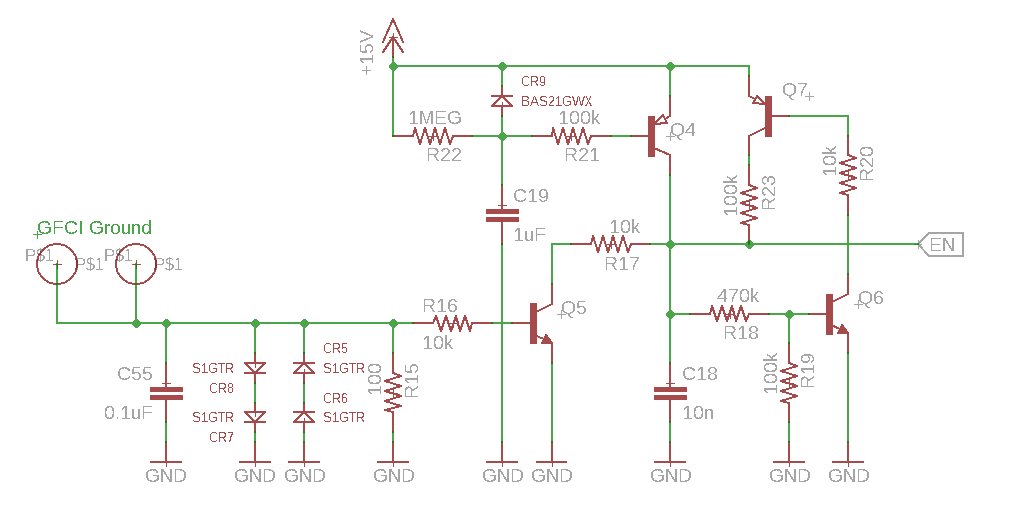
DC GFCI Circuit
GFCI circuits for houses typically work by using a transformer wound to detect unequal currents. Since this inverter has a DC output, such a circuit would not work. Instead, I chose to bond GFCI ground (The case of the inverter and the center pin of the NEMA5-15 outlets) to battery ground through two diodes in parallel with a resistor. Because diodes have a forward voltage drop, I would be able to detect leakage currents down to less than a mA. The resistor allows the minimum threshold of the circuit to be set so that tiny leakage currents don't cause the converter to shut down. Whenever the voltage of the GFCI node exceeds the base to emitter turn on voltage of Q5, that transistor begins to discharge the enable capacitor. If the enable voltage drops below ~3.6V, Q6 turns off which turns Q7 off. Q7 keeps the enable node charged, so with this transistor off the enable node latches in the off state.
In order to power up with enable high, Q4 initially charges the enable node at power up. After C19 charges, no further current will flow into the enable node from it until power is removed and applied again. A reset input could be added by connecting a momentary switch across C19. When C19 is shorted out, current will flow through Q4 again and the enable node will be recharged.
Full Bridge
The 170V bus voltage has to be chopped up at high frequency in order to generate a sine wave output. This is accomplished by a standard full bridge of N-Channel MOSFETs driven by half bridge drivers. A high PWM frequency is desireable since it allows for a smaller output filter, but higher PWM frequencies require higher microcontroller clock frequencies. The frequency of a PWM output directly scales with the resolution of that PWM output and the clock frequency of a microcontroller. A ATMEGA 328P has a standard clock frequency of 16 MHz, and an 8 bit PWM output requires 256 clock cycles per PWM period. This results in a maximum PWM frequency of 62.5 kHz which is pretty low. Additionally, the times at which the duty cycle of the PWM output is adjusted must be carefully controlled for accurate frequency output.
Due to these requirements, I decided to use an STM32F103 as the microcontroller on this project. It has a 72 MHz clock and a multiple highly capable timers. I was able to attach four digital outputs to the timer1 perifferal. The LA output is the complement of the HA output and the LB output is the compliment of the HB output. HA produces a PWM modulated half sine wave and then stays low during the other half cycle. HA does the same thing but is low while HA is producing a half sine as shown in the simplified chart below.
I took advantage of the Stm32duino libraries that have been developed for this part. Ideally, you would develop for the part using the ST provided standard periferal libraries, but I do not program on a daily basis, so I went with something that was easy to pick up. The only difficult aspect fo programming the part was determining how to enable the complimentary outputs. This part also supports programmable dead time, but I took the easy wasy out with that and selected half bridge drivers that insert deadtime and expect overlapping high and low drive signals like this.
Below is the full code required to get the STM32F103 to output the PWM signals needed to drive the full bridge to produce a sine wave:
#define HA PA8       //PWMA output (timer1 channel 1)
#define LA PB13      //complementary output
#define HB PA10      //PWMB output (timer1 channel 3)
#define LB PB15      //complementary output

int A_LUT[256]={0,6,12,18,24,30,36,42,48,54,60,66,71,77,83,89,94,100,105,111,116,121,126,132,137,142,146,151,156,161,165,169,174,178,182,186,190,
194,197,201,204,208,211,214,217,219,222,224,227,229,231,233,235,236,238,239,241,242,243,243,244,244,245,245,245,245,245,244,244,243,242,241,240,
239,237,236,234,232,230,228,226,223,221,218,215,212,209,206,203,199,196,192,188,184,180,176,172,167,163,158,154,149,144,139,134,129,124,119,113,
108,102,97,91,86,80,74,68,63,57,51,45,39,33,27,21,15,9,3,0,0,0,0,0,0,0,0,0,0,0,0,0,0,0,0,0,0,0,0,0,0,0,0,0,0,0,0,0,0,0,0,0,0,0,0,0,0,0,0,0,0,0,
0,0,0,0,0,0,0,0,0,0,0,0,0,0,0,0,0,0,0,0,0,0,0,0,0,0,0,0,0,0,0,0,0,0,0,0,0,0,0,0,0,0,0,0,0,0,0,0,0,0,0,0,0,0,0,0,0,0,0,0,0,0,0,0,0,0,0,0,0,0,0,0,
0,0,0,0,0,0,0,0,0,0,0,0,0};

int B_LUT[256]={0,0,0,0,0,0,0,0,0,0,0,0,0,0,0,0,0,0,0,0,0,0,0,0,0,0,0,0,0,0,0,0,0,0,0,0,0,0,0,0,0,0,0,0,0,0,0,0,0,0,0,0,0,0,0,0,0,0,0,0,0,0,0,0,
0,0,0,0,0,0,0,0,0,0,0,0,0,0,0,0,0,0,0,0,0,0,0,0,0,0,0,0,0,0,0,0,0,0,0,0,0,0,0,0,0,0,0,0,0,0,0,0,0,0,0,0,0,0,0,0,0,0,0,0,0,0,0,0,3,9,15,21,27,33,
39,45,51,57,63,68,74,80,86,91,97,102,108,113,119,124,129,134,139,144,149,154,158,163,167,172,176,180,184,188,192,196,199,203,206,209,212,215,
218,221,223,226,228,230,232,234,236,237,239,240,241,242,243,244,244,245,245,245,245,245,244,244,243,243,242,241,239,238,236,235,233,231,229,227,
224,222,219,217,214,211,208,204,201,197,194,190,186,182,178,174,169,165,161,156,151,146,142,137,132,126,121,116,111,105,100,94,89,83,77,71,66,60,
54,48,42,36,30,24,18,12,6,0};

int count=0;

void setup()
{
  HardwareTimer timer3=HardwareTimer(3);
  timer3.setMode(TIMER_CH1, TIMER_OUTPUT_COMPARE);
  timer3.pause();
  timer3.setCount(0);
  timer3.setPrescaleFactor(18);
  timer3.setOverflow(255);
  timer3.setCompare(TIMER_CH1, 100);
  timer3.attachCompare1Interrupt(handler);
  timer3.refresh();
  timer3.resume();

  HardwareTimer timer1=HardwareTimer(1);
  timer1.setOverflow(255);
  pinMode(HA, PWM);
  pinMode(LA, PWM);
  pinMode(HB, PWM);
  pinMode(LB, PWM);

  timer_dev *t = TIMER1;
  timer_reg_map r = t->regs;

  bitSet(r.adv->CCER,0); //this should enable complimentary outputs
  bitSet(r.adv->CCER,2);
  bitSet(r.adv->CCER,8); //this should enable complimentary outputs
  bitSet(r.adv->CCER,10);
}

void loop()
{
}

void handler(void)
{
  pwmWrite(HA, A_LUT[count]);
  pwmWrite(HB, B_LUT[count]);
  count++;
  if(count>255)
  {
    count=0;
  }
}
I realized after coding it up the first time that I could reduce the size of the lookup table by a factor of eight since the first quarter of a sine wave can be shifted and mirrored to produce everything else, but its not like I'm short on memory, so I didn't bother to change it. Note that there is no code in the main loop(). This is because everything the microcontroller is currently programmed to do is timer driven. Since I included resistor dividers to measure the input and output voltage of the boost converter, I will probably end up adding code here to measure the output voltage and disable the full bridge during prolonged brownout conditions.
There is a Chinese ASIC, EG8010, that is able to generate these waveforms, but I don't feel confortable using a part that isn't available on Digikey to control a high power device like this. There are modules based on this part for sale on Ebay that include gate drivers, but running gate drive traces through a pin header is pretty sloppy.
Output Filter
In order to attenuate most of the switching noise, a pretty agressive filter is required. I chose a 1mH 1uF LC low pass filter with a cutoff frequency of ~5.2 kHz. I did not find very much information online on what typical values for these filters are. I used a large inductor and a small capacitor so that the current circulating through the capacitor on every switching cycle was minimized.
Test Results
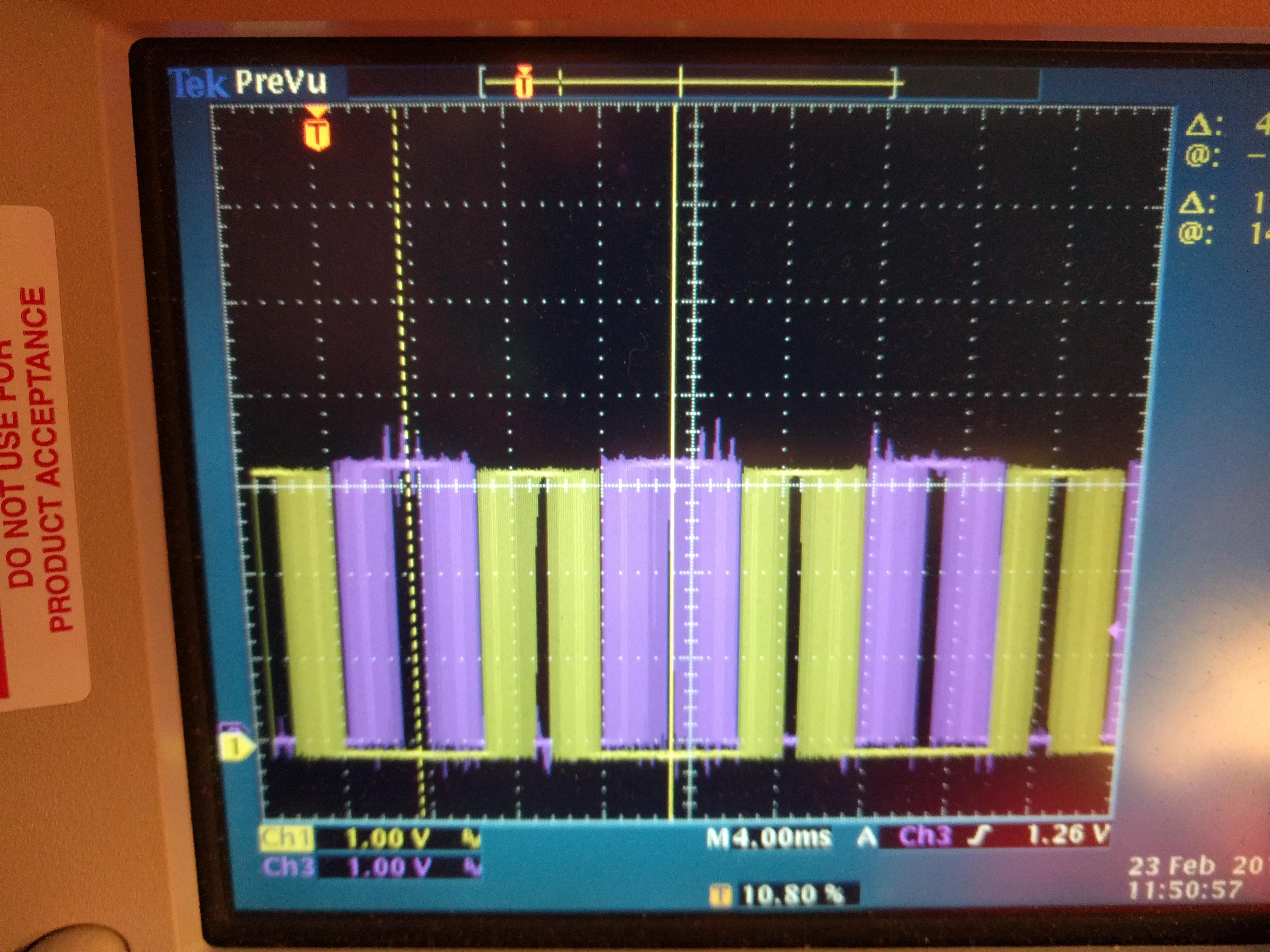
HA and HB PWM Signals
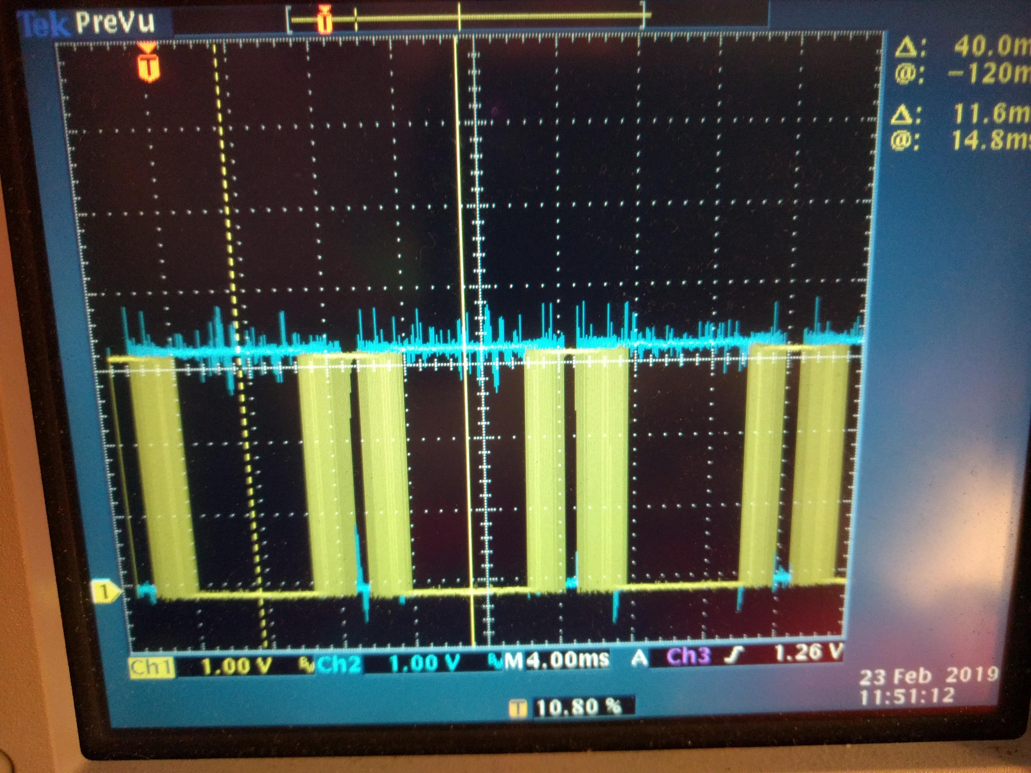
HA and LA PWM Signals
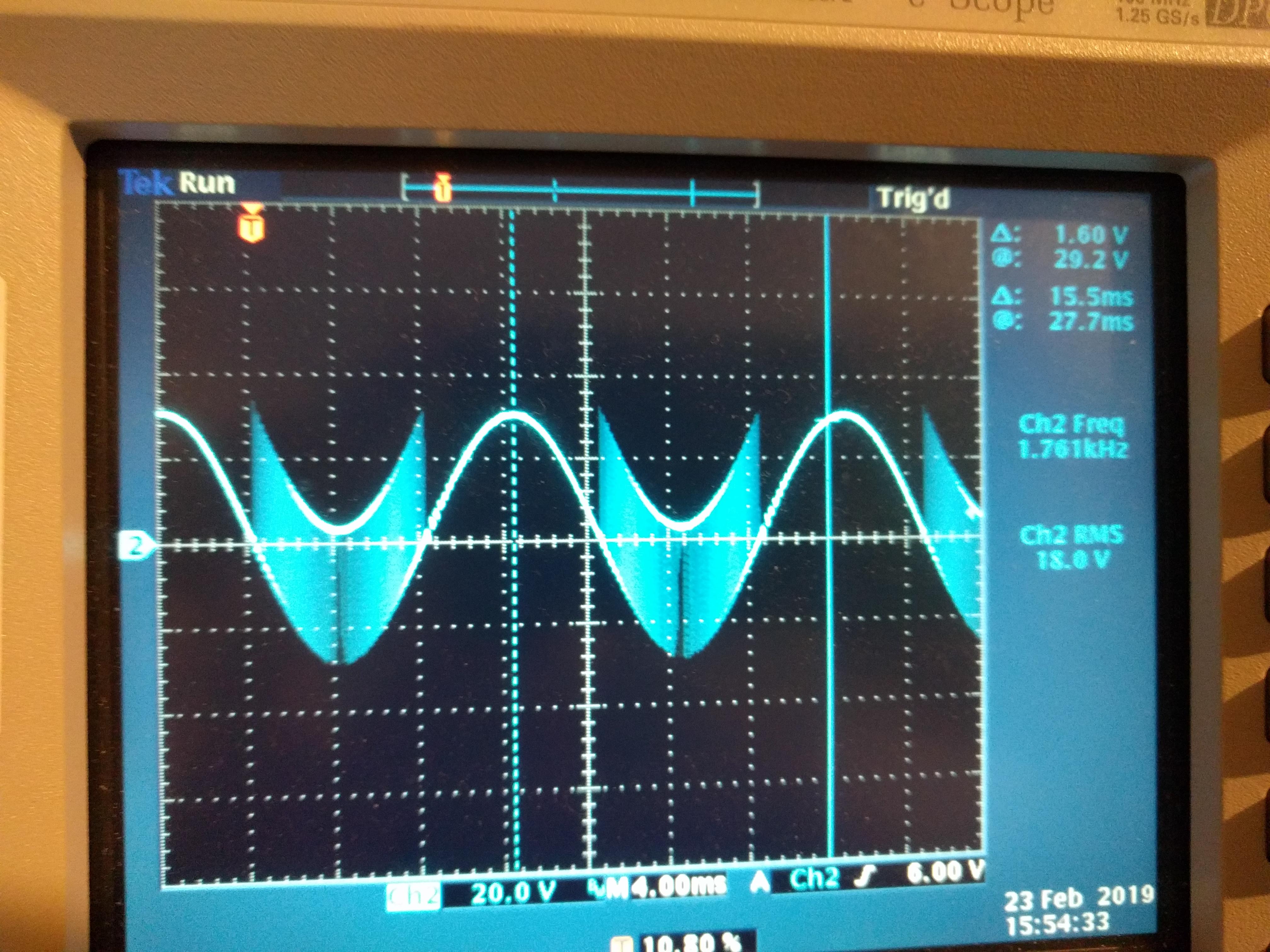
Intermediate Bus Ground Referenced Ouput A
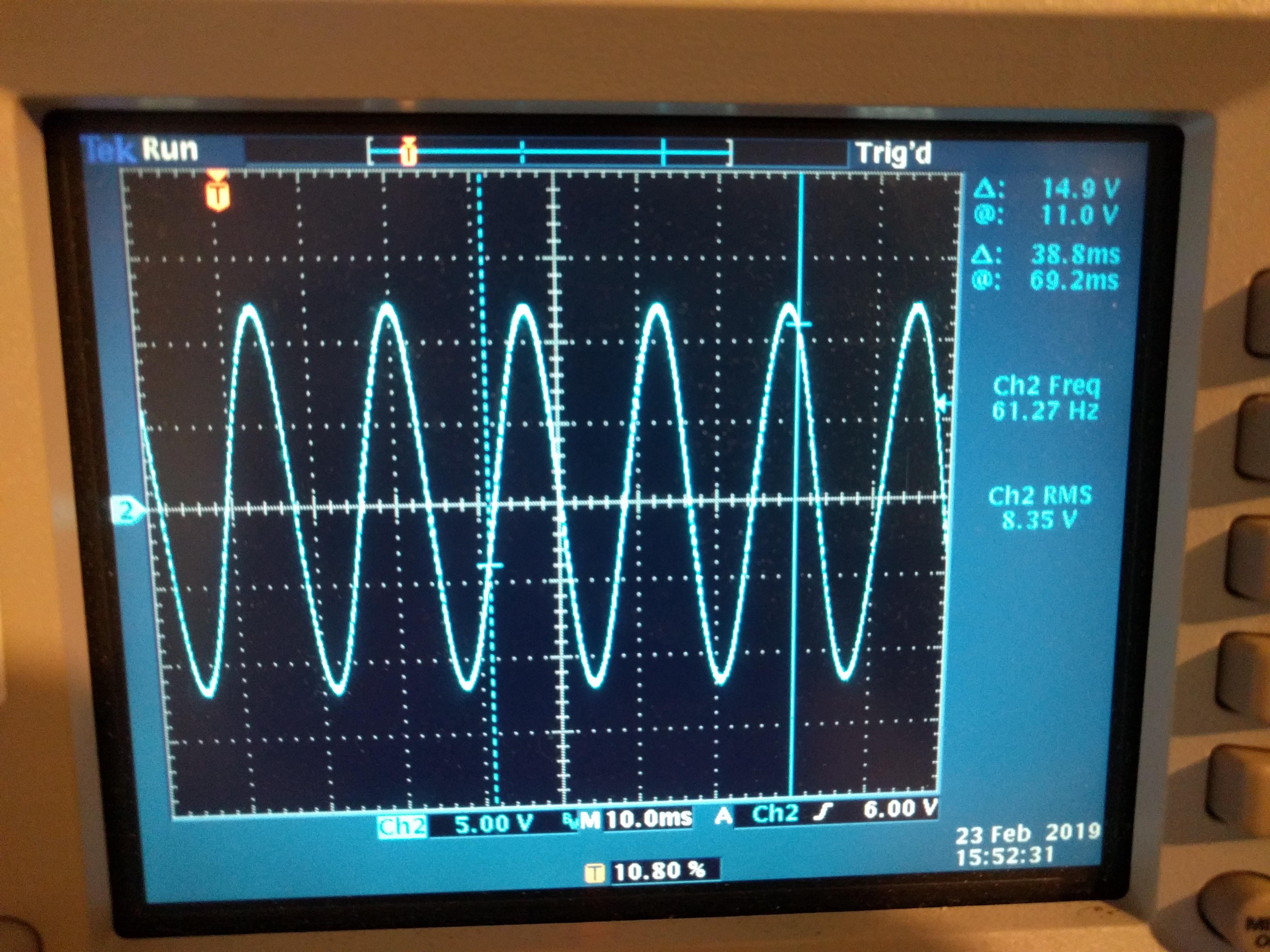
Output A Referenced to Output 2
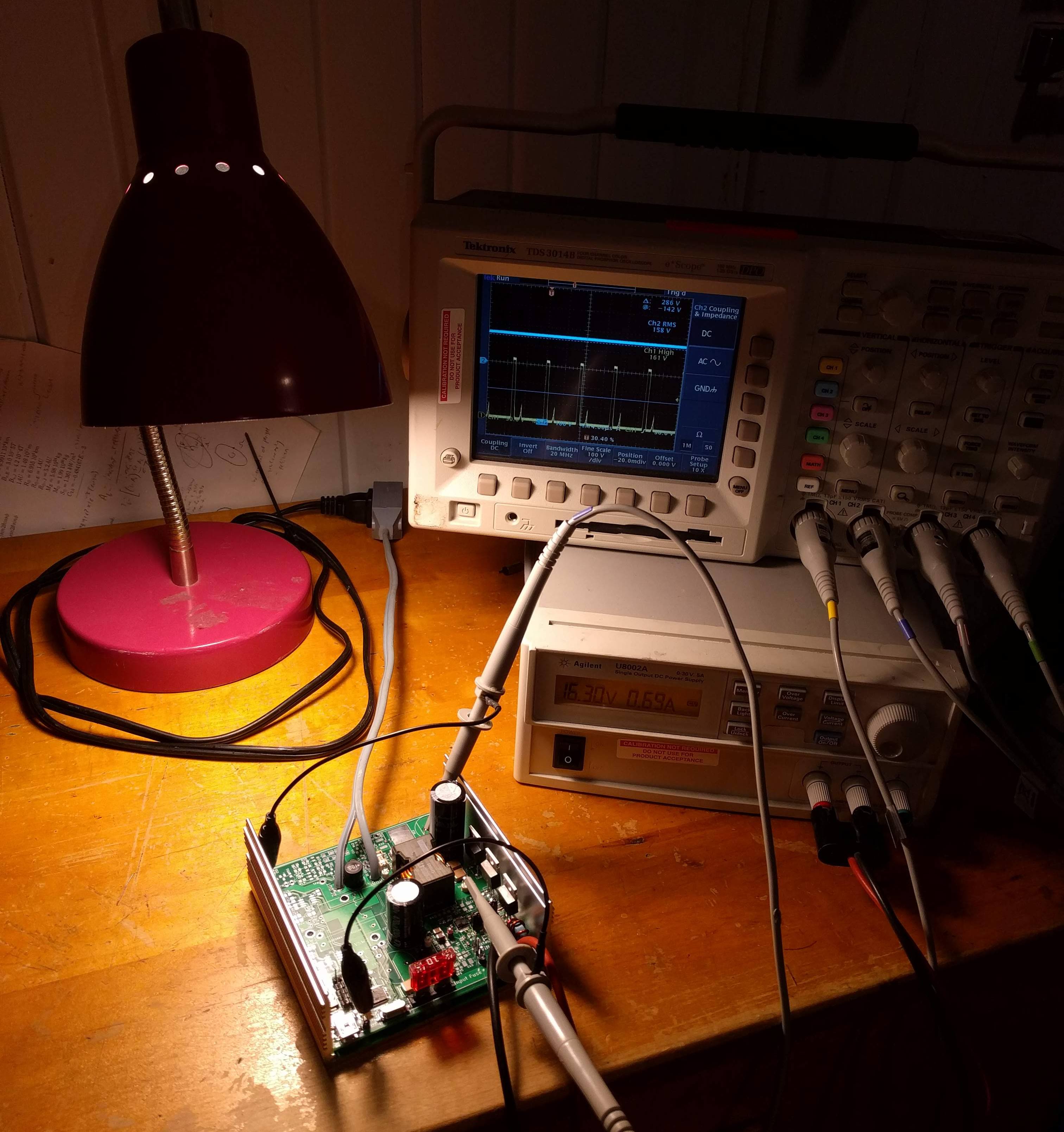
Test with LED Desk Lamp
Cheap and Easy Mounting Clamp
Bad Information and Commercial Inverters
There is a lot of bad information on power inverters online. If you search for power inverter schematics, you are likely to find a push pull circuit with two mosfets driving a center tapped transformer. This, however, is not what you will find in basically any comercial power inverter. 60 Hz transfrmers are heavy and expensive, and the leakage inductance of typical transformers will cause large voltage spikes on the inactive leg of the push pull that will need to be snubbed.
A typical comercial power inverter uses a small high frequency push pull converter to generate the high voltage rail and two half bridges like my inverter to generate the modified sine wave or pure sine wave output. A boost converter like I used is not well suited for 12V inputs due to the large conversion ratio. This results in more costly magnetics to get the job done which is not acceptable for a cost optimized commercial design.