Picoammeter
2021
Rev4 SchematicRev4 Layout
Rev4 EagleCAD Files
Normally when you measure current, you can ignore things like the input bias and input leakage of your measurement circuitry. When you need to measure picoamps, non-idealities like input leakage and input bias current can cause large measurement errors. One situation where you need to measure currents in the picoamp range is in nuclear detection with ionization chambers. I wanted to see if I could use gas discharge tubes to measure the flux of proton beams, so to test this idea out, I built a picoammeter. Beyond nuclear detection, picoammeters are also useful for measuring the leakage of semiconductor devices and insulators.
Most of the circuits you can find online for ionization chambers are based on discrete transistors and don't provide fantastic linearity or accuracy. The picoammeter circuit based on LMC662 that gets passed around DIY forums works acceptably (and my first prototype was a close copy of it), but I wanted to see how to improve its performance without using significantly more expensive parts. Ultimately, I settled on LMP2231 as the best balance of cost and datasheet guaranteed DC performance. Optimizing for AC performance is a different ballgame (who cares about DC when you're AC coupled) that I had to deal with when I modified this circuit to measure current from alpha particles hitting a photodiode.
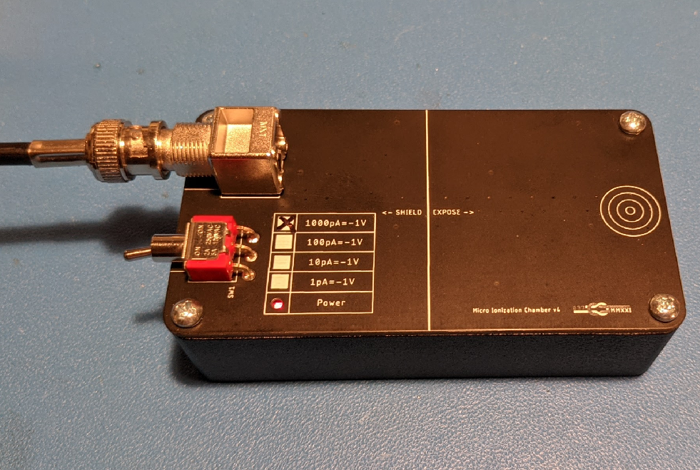
Combined Picoammeter and Ionization Chamber
How to Measure Tiny Currents
Multifunction devices capable of measuring very small currents, very high resistances, and charge are called elecrometers. I am just interested in instantaneous current, so it is just the picoammeter functionality of an electrometer that I need to replicate. There are three general types of current sensors with the necessary sensitivity to measure picoamp and nanoamp range currents:
- Shunt Ammeter
- Feedback Ammeter (Transimpedance Amplifier)
- Coulombmeter
Shunt Ammeter
Ordinary shunt current sensors will work, but there are major downsides. If you place a 1MΩ resistor in series with a 1pA current source, you'll only get 1uV. Up that to 1GΩ, and you'll get 1mV. That is certainly a voltage that a sensitive amplifier can deal with (ignoring input impedance and bias issues discussed later), but you run into problems when you also need to sense larger currents. A 1nA current produces 1V across the shunt which means that the voltage across the DUT is 1V lower which will impact the measurement if the current through the DUT is voltage dependent. This voltage drop is known as burden voltage.
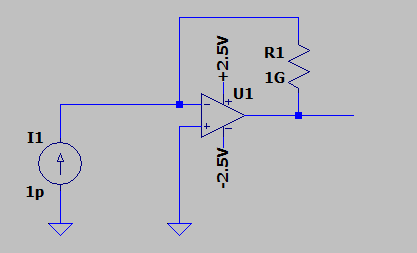
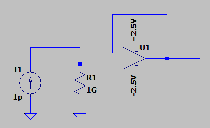
Transimpedance Amplifier
The solution to this problem is to place the resistor in the feedback path of an OP-AMP. For a given resistance, current to voltage gain is the same as with a shunt current sensor, just inverted because the OP-AMP must lower its output voltage in order to keep its inverting input at a constant voltage despite current being injected into that node by the DUT. Because the OP-AMP keeps its input voltage constant, the voltage across the DUT can be held constant. Feedback ammeter is a term used in the Keithly Low Level Measurements Handbook, but a more general term is Transimpedance Amplifier (TIA). This type of circuit is often used as a first stage amplifier in photodiode circuits.
Coulombmeter
Coulombmeters measure electric charge, not current, but they can act as discrete time current sensors and can provide very good resolution. These can also be implemented as shunt and feedback circuits: shunt coulombmeters monitor the voltage produced by the DUT charging a capacitor, and feedback coulombmeters place that capacitor in the feedback network of an OP-AMP. The problem with coulombmeters is that they must be reset after their amplifiers rail out when their output reaches a supply rail. Any reset circuit connected to the input of the amplifier must have extremely low leakage in the off state. For reasonable performance, the reset circuit must use an electromechanical relay. "Low leakage" MOSFETs still have leakage currents >10nA with only a volt or two drain to source, so mechanical relays are typically used in sensitive electrometer applications for resetting integration capacitors, reconfiguring circuitry and changing gain values.
Limits to Precision
There are three main contributers to DC error in transimpedance amplifiers: feedback resistor tolerance, OP-AMP input bias current, and OP-AMP input offset voltage. I found that LMP2231 had the best balance of these parameters for this application despite its relatively low cost ($1.70).
Feedback Resistor
1GΩ is the largest value resistor that can be purchased for less than $1 with a 1% tolerance:
- 1GΩ 2512 1%: $3.30
- 2GΩ 0805 1%: $11.00
- 1GΩ THT 1%: $0.79
- 5GΩ THT 1%: $3.93
A 10GΩ resistor would provide even more sensitivity, but it would add cost.
Input Bias Current
Input bias current is the parasitic current that flows into or out of the input of an OP-AMP. Zero current flows into the inputs of an ideal OP-AMP, and this aspect of OP-AMPs can generally be treated as ideal in lower impedance circuits, but wherever there is a voltage potential in real circuits, some leakage current will flow. In a CMOS OP-AMP, most of this current is from the ESD protection diode structures. Input bias current is common mode voltage dependent because the effective input bias current is the sum of the leakage from the top side and bottom side ESD diodes. With identical ESD diodes, you would expect the common mode voltage that corresponds to zero leakage to be at half the supply voltage since the reverse voltage across each ESD diode would be the same. Real parts have variation, so while you can reduce input bias current by adjusting your common mode voltage, you cannot eliminate it across temperature.
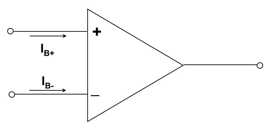
Input Bias Current
Since input bias current effects both inputs to an OP-AMP, much of its effect can be cancelled out by connecting both inputs to nodes of similar impedance. What cannot be compensated for with this method is input offset current -- the difference between the input bias currents of the two inputs. If both inputs are sinking 1pA with a 1GΩ source impedance, the voltage at both input nodes will be 1mV lower canceling out the effect. If one input is sinking 1pA and the other is sinking 1.1pA, then there will be a 100uV difference in voltage at the two pins. Assuming a TIA circuit, the output voltage would then have a 100uV offset.
LMP2231 has typical input bias current of 0.02pA and a typical input offset current of 0.005pA. Those parameters only hold at 25C die temperature and with a common mode input voltage of half the supply. The maximum input bias current (inclusive of all input common mode voltage and operating temperatures) is 2500x higher: 50pA. From the performance characteristics plots, you can see how common mode voltage impacts input bias current:
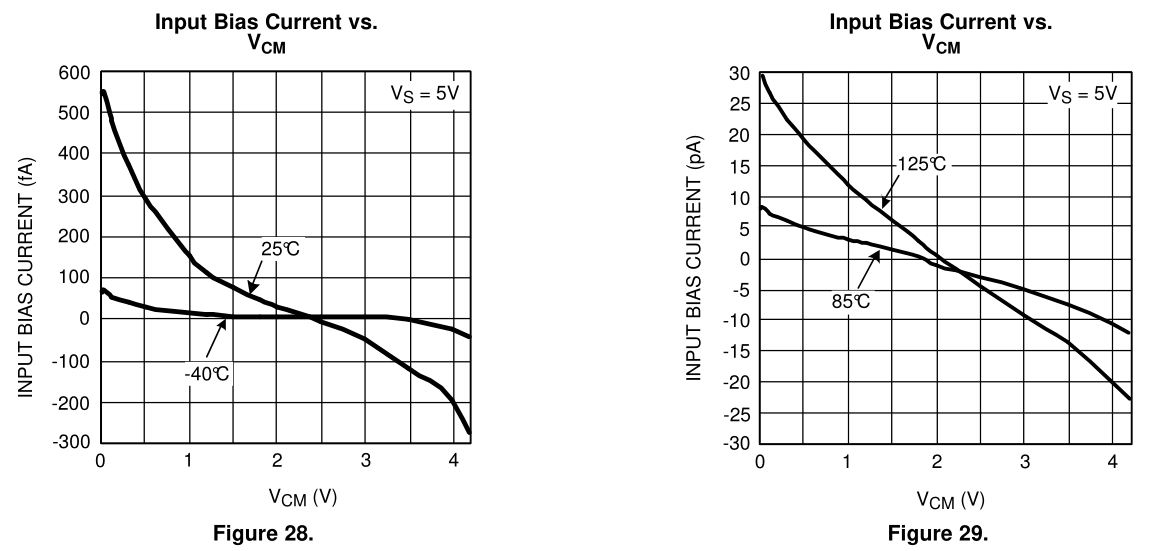
LMP2231 Input Bias Current vs. Common Mode Voltage Over Temperature
With a common mode voltage of 0V (as you would have with a typical shunt ammeter in a system without negative supply rails), the input bias current at 25C can be more than 0.5pA which is 25x the value listed in the datasheet for 'typical' input bias current. Thus, the feedback ammeter topology has significant benefits beyond just eliminating burden voltage since it inherently maintains a constant non-zero common mode voltage. For this particular amplifier, the best common mode voltage for operation over a wide temperature range is 2 Volts. Input offset current (the difference in input bias current for the two inputs)for this device is so low that it was likely impractical for the manufacturer to characterize it, but assuming that it can be modeled as a percentage of input bias current added to a constant offset, it should be minimized at the minimum input bias current point as well.
I did not bother matching the input impedances for my initial circuit, and at room temperature for how I use the sensor it is not really required. The output voltage with only background radiation the output voltage is 0.0mV which is as low as my Fluke multimeters go. If this sensor were to be used over a wide range of temperatures, it would be wise to match input impedances, though. The theoretical output offset resulting input offset current in a matched impedance circuit is equal to the input offset current multiplied by the feedback resistance. So for a 0.005pA offset and a 1 GΩ feedback resistor, the typical offset should be 5uV which is of course far below the 100uV sensitivity of my multimeter.
Input Offset Voltage
Input offset voltage is the difference in voltage that can be measured between the two inputs of an OP-AMP. This offset is the result of mismatch in the input transistors of the OP-AMP and the circuits that bias them. Input offset is a function of temperature, but the nominal value can vary significantly on a part to part basis. The temperature coefficient also varies significantly between parts: LMP2231A is screened to have a maximum temperature dependent drift in input offset voltage of +-0.4uV/C while LMP2231B may have a value as high as +-2.5uV/C. Since I am using this part at room temperature, I opted for the cheaper LMP2231B.
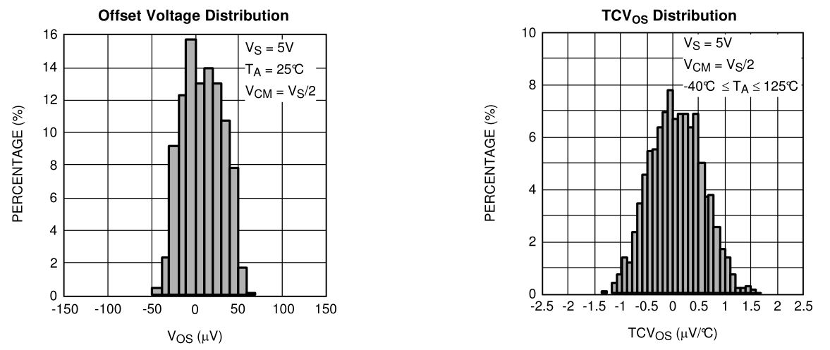
LMP2231 Input Offset Voltage Distribution
In a proper electrometer, input offset voltage is compensated for in a calibration step, but temperature dependent drift can still cause issues if the electrometer changes temperature during operation without recalibration.
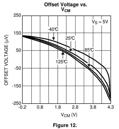
LMP2231 Input Offset Voltage vs. Common Mode Voltage Over Temperature
As with input bias current, there is a sweet spot in common mode voltage for input offset voltage. In this case, it is around 3V. This voltage is a bit higher than the sweet spot for bias current, so the ideal common mode voltage depends on the range of temperatures over which the detector needs to operate. I elected to use a 2.5V common mode voltage because it is exactly half rail and is an average of the ideal common mode voltage for input bias current and ideal common mode voltage for input offset voltage.
Implementation
LMP2231 is only rated to 5.5V, so I added a 5V linear regulator to allow the circuit to be powered off of a 9V battery. There is nothing special about the linear regulator -- I just chose whatever I already had in my library.
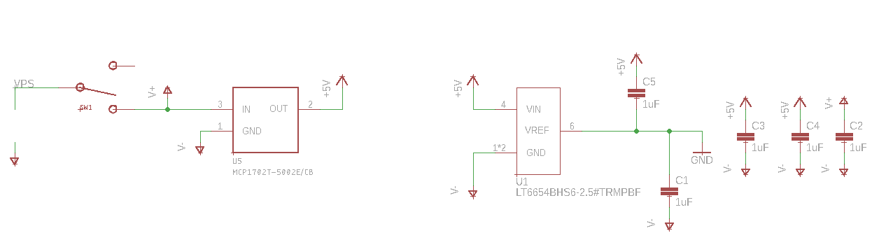
Power Supply for Picoammeter
Feedback ammeters use split rail power supplies. The output voltage is not referenced to the negative supply pin -- it is referenced to the virtual ground of the common mode input. This virtual ground can be created by buffering a resistor divider between the positive and negative supply and that works fine for battery operated applications where nothing outside the circuit sees the negative supply, but there are issues when you want to measure the output voltage with a device referenced to the negative supply like an ADC. You could measure both the virtual ground and the output of the TIA and subtract the two, or you can use the virtual ground as the reference of the ADC so that all reading are inherently referenced to virtual ground. Since the accuracy of a virtual ground formed by a rail splitter circuit is only as good as the tolerance of the positive rail supply and the resistors in the resistor divider, I instead chose to use the output of a 2.5V reference as the virtual ground. LT6654 is a 0.1% reference with a high output drive which supports output capacitors in excess of 1uF, so it is ideal for this application.
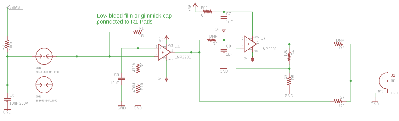
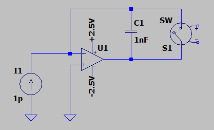
Picoammeter Circuit
Because of the very high gain of this circuit, it is necessary to add a capacitor across the feedback resistor to prevent oscillation. This needs to be a very low leakage capacitor because any leakage will throw off the gain accuracy of the picoammeter. I started with a 47pF film capacitor which works fine for inherently slow changing devices like ionization chambers, but to measure fast events like single particles hitting a photodiode, it is necessary to use a lower value. The minimum value is determined by this stability equation:
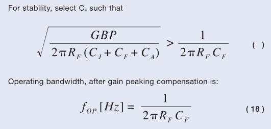
Stability Equation from OSI Optoelectronics App Note
For very low value capacitors in low frequency circuits like this, you can get away with twisting two wires together and calling that a capacitor. The term of art for this hacky solution is Gimmick Capacitor. I untwisted the capacitor a quarter inch or so at a time until the circuit became unstable, and then then retwisted and trimmed.
Simulation
LTSPICE will misbehave at currents and voltages in the pA range, but it seems to do alright as long as sources reach the nA range during the simulation.
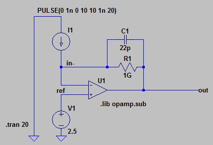
Simulation Schematic
Here is the predicted output voltage across a sweep of input voltage:
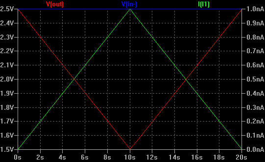
Simulation Result
Layout and Shielding Considerations
I did not understand how exceptionally sensitive to outside noise circuits with 1GΩ input impedance were until this project. I designed the circuit as a lid for an aluminum box mostly convenience, but that ended up being a critical choice. Without the box, the circuit is totally unusable due to electric field coupling from AC mains.
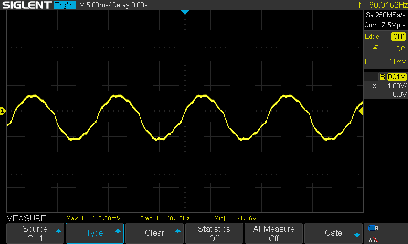
Output without the Box Screws Installed
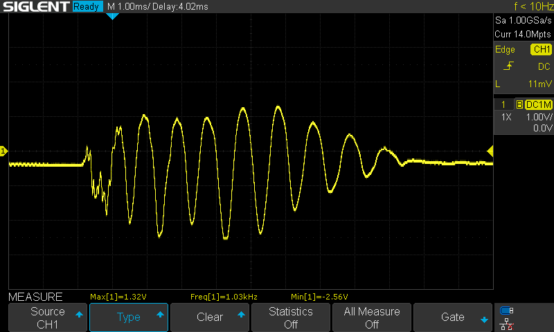
Touching a screwdriver to the auxiliary input of the Rev2 design results in the amplifier railing out:
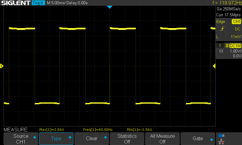
Output While Touching the Input
Even holding a finger near the auxiliary input without the resistor inside that connects the aux input to the op-amp installed was enough to get a clear response. This is just capacitive coupling through my body to the input connector and then capacitive coupling across the pads of the DNP resistor. This effect is seen even though there is a guard trace running in between the pads of this resistor.

Auxiliary Input Layout that Still Influences Circuit When R4 is DNP
All high impedance traces in circuits must be surrounded by guard rings to prevent leakage and noise coupling. The guard ring is connected to the non-inverting amplifier input (the virtual ground produced by the voltage reference), so it is kept at the same nominal voltage as the sensitive input node. All of the ground planes are connected to the virtual ground instead of the negative battery terminal. The metal box is also tied to the virtual ground by the four corner mounting holes.
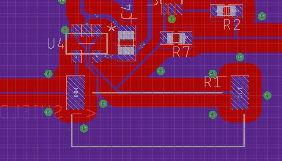
Guard Trace (red dashed line) Around Inverting Input
The circuit is also sensitive to vibration like from tapping the box with the handle of a screw driver:
Output from Tapping Box with Screwdriver Handle