USB Power Bank
2022
SchematicLayout
Rev4 EagleCAD Files
STL Files for Case
After discovering that disposable vapes contain rechargeable lithium ion cells, I thought it would be fun yo build a USB power bank using those cells. I had most of the parts in my library already (I only needed to create the boost converter part), so I was able to throw this full design together in about three hours. When I sat down to write this up, I though: "Huh. This is a lot of parts. Someone has to have made an IC that handles all of this." Well, it turns out that they have. I could have replaced every IC on this board with MP2696, and astonishing that part even has stock on Digikey in the middle of the COVID/post-COVID parts shortage. Several of the other parts on the board had no distribution stock, but I had them in my parts box from previous projects. The MP3423 boost converter actually went out of stock right after I ordered, so I can't build any more of these for the foreseeable future even if I wanted to.
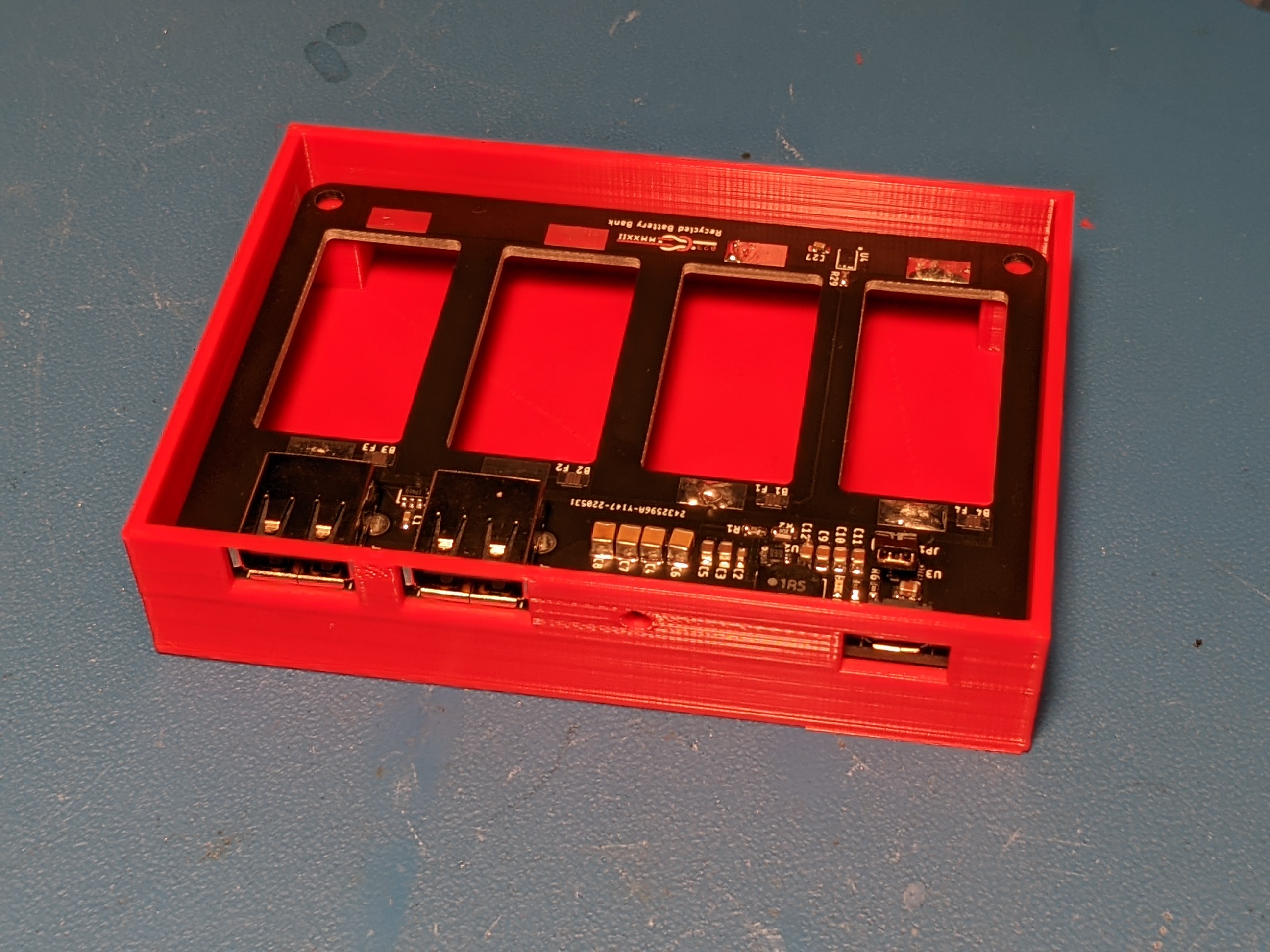
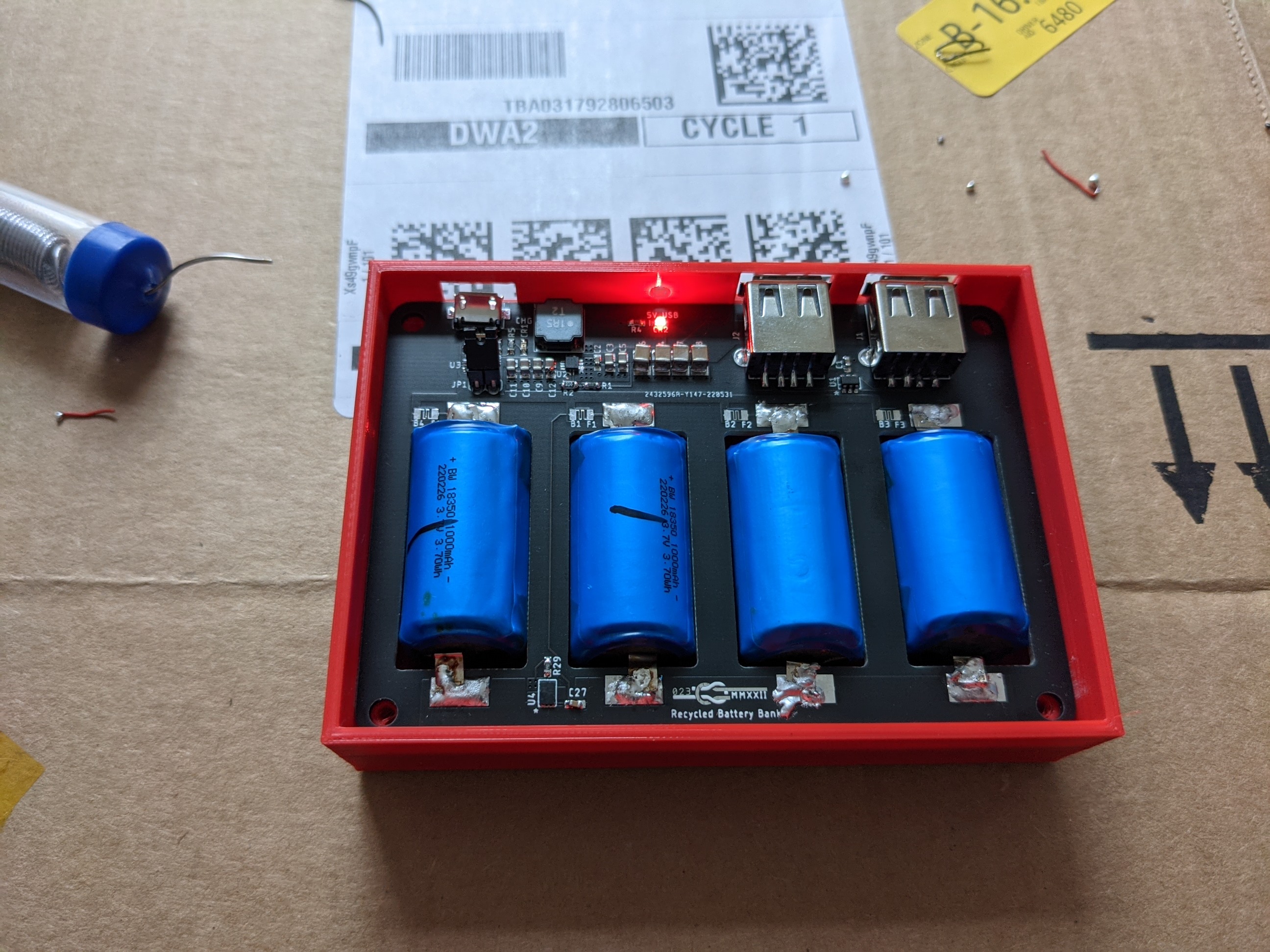
Assembled Board In 3D Printed Case
This project is an unabashed exercise in "app-note engineering". That is, often said pejoratively, implementing the example design in IC data sheets and application notes without applying any deeper thought. When you need to whip up a quick solution to a problem that will have limited production volume, "app-note engineering" is often the correct engineering trade off between cost of engineering time and cost of an overkill or unoptimized solution. You can get pretty far in engineering by regurgitating what you find in data sheets, but, without a first principles understanding of what each of these circuits is doing, you'll find yourself in a tough situation if you need to deviate from the operating points in the example circuits.
Circuit Breakdown
A USB power bank needs to handle a couple functions:
- Charging the Lithium Ion Cells from a USB Source.
- Protecting the Lithium Ion Cells against Over-Voltage, Over-Current, and Under Voltage.
- Generating 5V from the 2.7-4.2V Lithium Ion Cell.
- Detecting the presence of a device to be charged.
- Signaling to the device being charged the capabilities of the charger.
In my naive power bank implementation, a separate IC performs each of these functions aside from detecting the presence of a device to be charged which I elected to omit in favor of a manual switch.
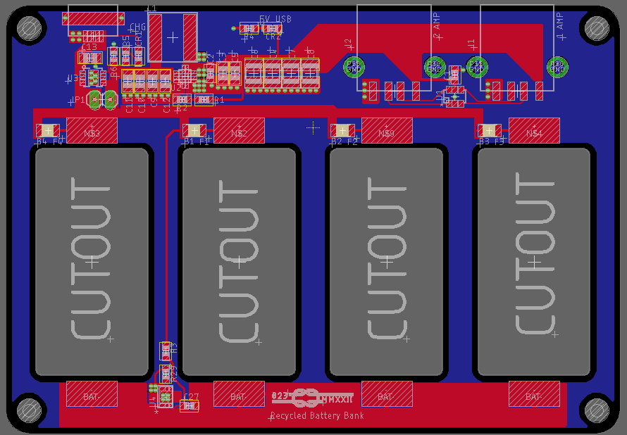
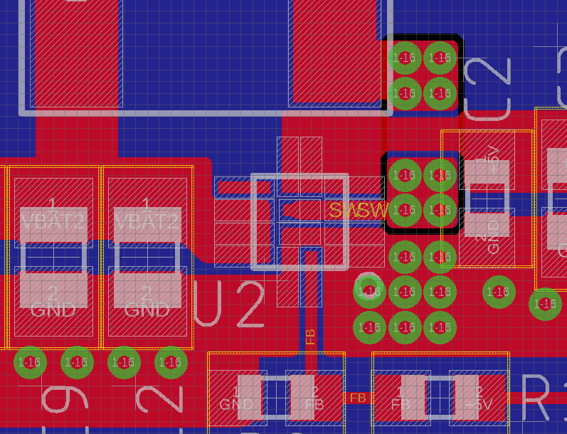
PCB Layout For Vape Cell Power Bank
Charging the Bank
USB chargers of lithium ion batteries are often implemented with linear circuits since power from USB ports is "free". In a cell phone, a switching supply is used to cut down on the dissipated heat and to support faster charge rates at higher USB-C voltages (9 or 12V often).
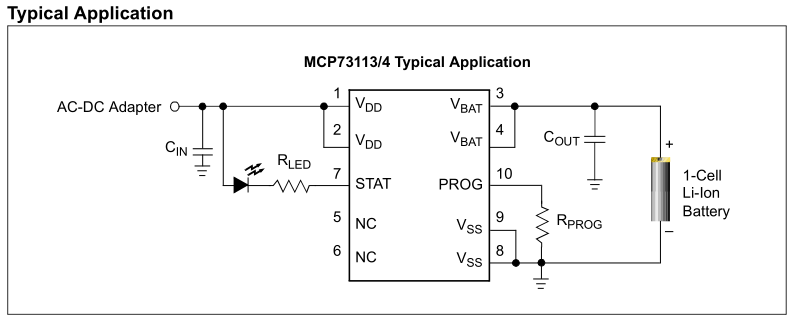
MCP73114 Application Circuit
Here, I used MCP73114 to charge the cells at around 600mA. There is no detection of the capability of the charger, but just about any USB 2.0 port (technically 'high power' USB 2.0 devices should not draw more than 500mA) and all USB 3.0 ports (900mA 'high power' device standard) will support a 600mA charge rate. With a 3V battery voltage, this charger is only 3/5=60% efficient, so the board does get quite warm while charging, but the part stays well within its temperature limits.

MCP73114 Charge Current Setting
To select a 600mA charge current, I used a 2kΩ charge current programming resistor.
Battery Protection
Lithium ion batteries can present a hazard (explosion, fire) if they are abused. Discharging a lithium ion battery below its minimum rated voltage (often 2.5-2.8V) will result in permanent loss of capacity and can cause the growth of dendrites within the cell that can short the entire battery out. Charging a battery above its maximum rated voltage (often 4.1-4.4V) can result in thermal runaway. MCP73114 provides primary protection against overcharge in that it will not charge past 4.2V, and AP9211 provides secondary protection. AP2911 also protects against under-voltage and overcurrent. In the event of a short circuit, it will keep the output off until the load is entirely removed.
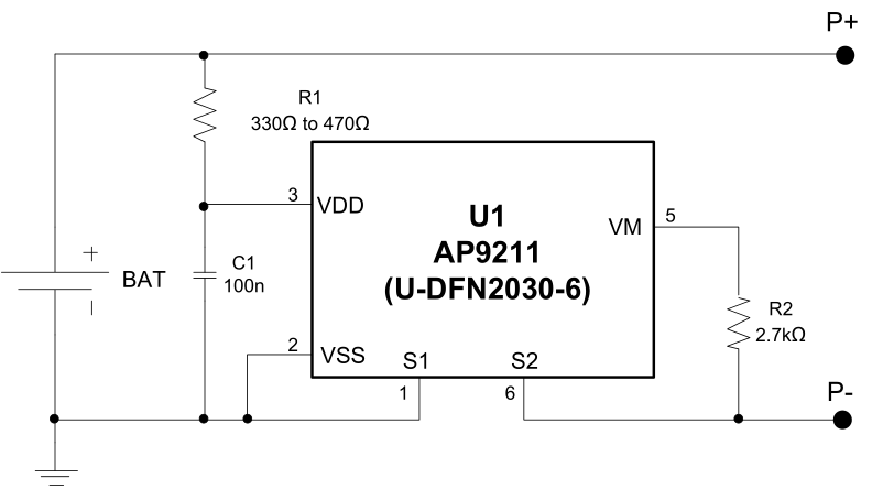
AP9211 Battery Protection IC
I chose AP9211 (specifically AP9211SA-AE-HAC-7) for a project a couple years ago because it is available with pretty conservative limits; many similar protection IC have under-voltage and over-voltage trip-points in excess of the typical rated voltages of lithium ion cells (less than 2.5V, greater than 4.2V). This part, of course, was out of stock when I designed this board, but I was able to reuse an old part that I de-soldered from a scrap board. The great parts shortage has legitimized hoarding habits in electrical engineers, and just as our grandparents kept drums full of old sour cream containers in the basement in response to their experience of scarcity in the great depression, electrical engineers are likely to hold on to their PCBA bone piles for some time to come as insurance against not being able to find even a single instance of a part that they need.

AP9211 Set-point Selection Table
Boost Converter
The switch current rating of a boost converter is not the same as its output current rating. If you are boosting 3V to 5V, you need (ignoring losses) 5A at 3V to generate 3A at 5V. That means that you need a boost converter with a switch current rating of greater than 5A to supply a 3A output. In May 2022, the only reasonable part that fit that description on Digi-key was MP3423. Monolithic Power Systems makes very dense and very efficient parts because they integrate everything onto the same die. Whereas other manufacturers may use a separate controller die and MOSFET die in the same package, MPS will integrate everything onto the same die. In this case, their 9A capable boost converter part fits in 2x2mm. The inductor is comparatively massive.
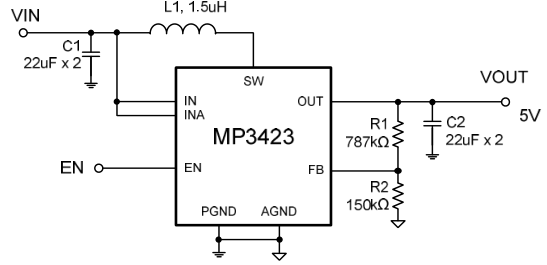
MP3423 Application Circuit
Being as small as it is, I modified the part footprint to extend the pads past the datasheet recommendations. With small QFNs like this, having additional pad length to contact with your soldering iron really helps to make sure that every pad is correctly soldered and that there are no shorts after reflow soldering without a stencil. My typical practice when hand soldering parts like this is to deposit solder paste on the pads, align the part well, reflow, and clean it up afterwards with flux and a soldering iron.
Extended Pads of MP3423 Footprint
The only issue I had with this board was the stability of this boost converter. When I initially assembled the board, I used feedback resistor values in the 10k range. It was unstable and exhibited subharmonic oscillation. I brooded for a bit and then realized that, since this is an internally compensated part, it may be sensitive to feedback resistor values. I read the datasheet, and sure enough, the part requires a top-side feedback resistor greater than 600kΩ in order to ensure stability. After changing the feedback network to have a 1MΩ top side feedback resistor, the converter ran great.
USB Dedicated Charging Port IC
A high power USB 2.0 device is only supposed to draw 500mA, but many USB wall chargers with USB-A ports will output 2-3A. In 2013 when I bought a Google Nexus 7 tablet, I found that it determined what rate to charge at based only on voltage. It ignored the data lines when they were not connected to a hist and, apparently, assumed whether it was good to draw additional current from a dumb charger based on voltage drop. I was a bit surprised to see that my Google Pixel 3 would only charge "slowly" (presumably at 500mA) from dumb chargers that don't drive the data lines such as my Leaf battery bank. To get devices to charge more quickly, you need to bias the USB data lines or short them out with a specified resistor. There are a class of devices called dedicated charge port (DCP) controllers that handle this task, and I selected Texas Instruments TPS2513 for this.
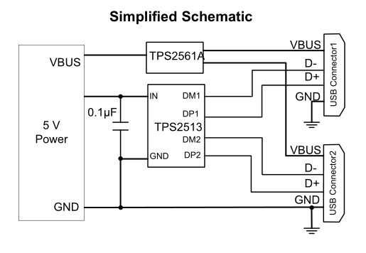
TPS2513 Reference Schematic
TI Data sheets are often not fantastic. Linear Technologies (now Analog Devices) sets the gold standard for data sheets with their rich application descriptions and examples, but TI sometimes leaves you guessing as to what each part variant even does. For this part, it took me a bit to catch that the way you are able to set a port to be 5W capable or 10W capable is by whether you reverse the USB data lines. If you connect them straight on TPS2513 (DM to DM and DP to DP), devices will; interpret the charger as a 10W charger and if you reverse the connection, devices will interpret the charger as a 5W charger. For my circuit, I set J2 as a 2A charger and J1 and a 1A charger.

TPS2513 Charge Current Configuration
The Value of Integration
As I mentioned in the introduction, all of the functionality of the previously mentioned parts can be implemented in a single IC. MP2696 implements all of the previous functionality, but it also implements temperature sensing, buck charging to lower charging losses, USB plug in detection, and I2C monitoring. This is a $1.50 part in quantity through Digi-key. The combined cost of the four ICs that I used is $3.55 through Digikey if you want to build 1000 of these banks. If I ever build something like this again, I will go with a more integrated solution like MP2696.
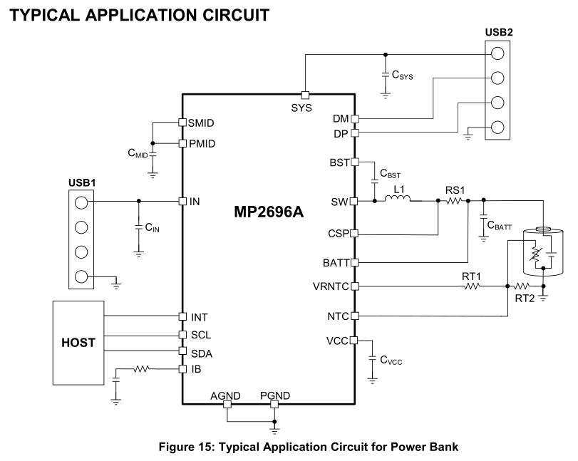
MP2696 Typical Application
Capacity
I measured the cells using a battery charger / discharger that I bought second hand in college for $20.
To my surprise, the capacity of the cell with a 1C (1A) discharge was 1,040 mAh which is 4% higher than the capacity listed on the side of the cell.
I tested the power bank with a single cell installed and was was able to charge my phone 34% before I hit UVLO (under voltage lock out).
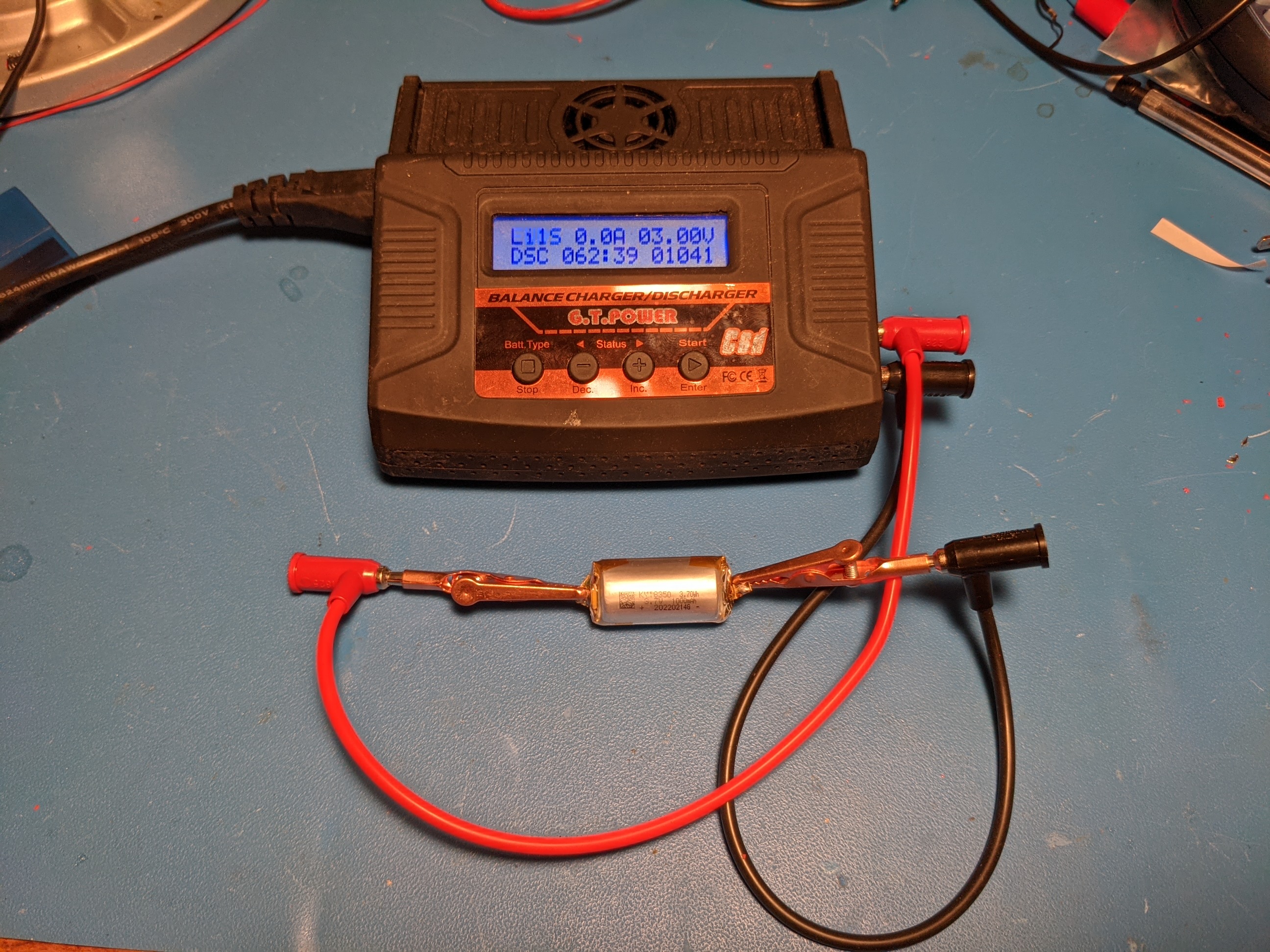
G.T. Power Charger/Discharger Discharging a Single Cell
The single cell also got pretty warm in the process since it was being discharged at around 3A. With all four cells installed, each cell will dissipate 1/16 the power of the cell in the single cell test. Cell losses are I^2R (current squared times internal resistance). With four cells, the current through each will be 1/4, and (1/4)^2 is 1/16. Total loss across the four cells is one quarter that of the single cell test since there are four cells each dissipating 1/16 the original power. As a result, I expect to get about 1.5 charges of my Google Pixel 4 out of this power bank.
Construction
Since these cells are tabbed, I put cutouts inside of the PCB to allow them to be 'mid-mounted.'
You are unlikely to see this in a commercial product since it is very inefficient of PCB laminate (the cutouts go into a landfill), but it is convenient when you are paying, arguably, loss leader prices from a Chinese fab house like JLC PCB, there is no cost benefit to making the board smaller than 100x100mm.
Lead Free Solder Results in my Messiest Work In Years
The case for the charger is 3D printed from PLA, so it will undoubtedly go up in flames if one of the cells ever pops off. The battery protection IC provides a current limit, but as a protection against a catastrophic event, I included 5-mil bare PCB trace fuses which should blow within a few seconds at 5A on each cell.
Assembled Box With Lid
To turn the bank on, you open the lid and install the jumper. Obviously this is not optimal, but it gets the job done. Integrated parts like MP2696 include circuits to detect attached loads which obviate power switches. Those circuits can have the side effect of enforcing an effective minimum load, though. I have run into this with power banks running, for example, low power LNAs for test applications. With a physical switch I at least have the flexibility to run low current loads without them cutting due to undercurrent.